Optical Wafer and Die Probe Testing

a technology of optical communication system and probe, which is applied in the field of integrated circuit testing, can solve the problems of low yield rate, inability to successfully extend the probe testing of integral wafer-contained circuit dies for electrical properties to electro-optical devices, and the existing solution for testing optical communication systems within ic chip devices is extremely difficult at a practical level

Inactive Publication Date: 2014-12-11
NXP USA INC
View PDF2 Cites 30 Cited by
  • Summary
  • Abstract
  • Description
  • Claims
  • Application Information

AI Technical Summary

Problems solved by technology

But with any integrated circuit technology, there are technical difficulties and challenges posed by fabricating such devices, including but not limited to lower yield rates that can result from manufacturing defects that can occur, especially as device geometries shrink, device performance increases, and fabrication technologies advance.
In addition, probe testing of integral wafer-contained circuit die for electrical properties has not been successfully extended to testing of electro-optical devices due to a number of challenges posed by generating, delivering, and processing optical test signals, as well as the additional die size requirements imposed by including optical test circuitry in the individual die.
As a result, the existing solutions for testing optical communication systems within IC chip devices are extremely difficult at a practical level.

Method used


Image

  • Optical Wafer and Die Probe Testing
  • Optical Wafer and Die Probe Testing
  • Optical Wafer and Die Probe Testing

Examples


Embodiment Construction

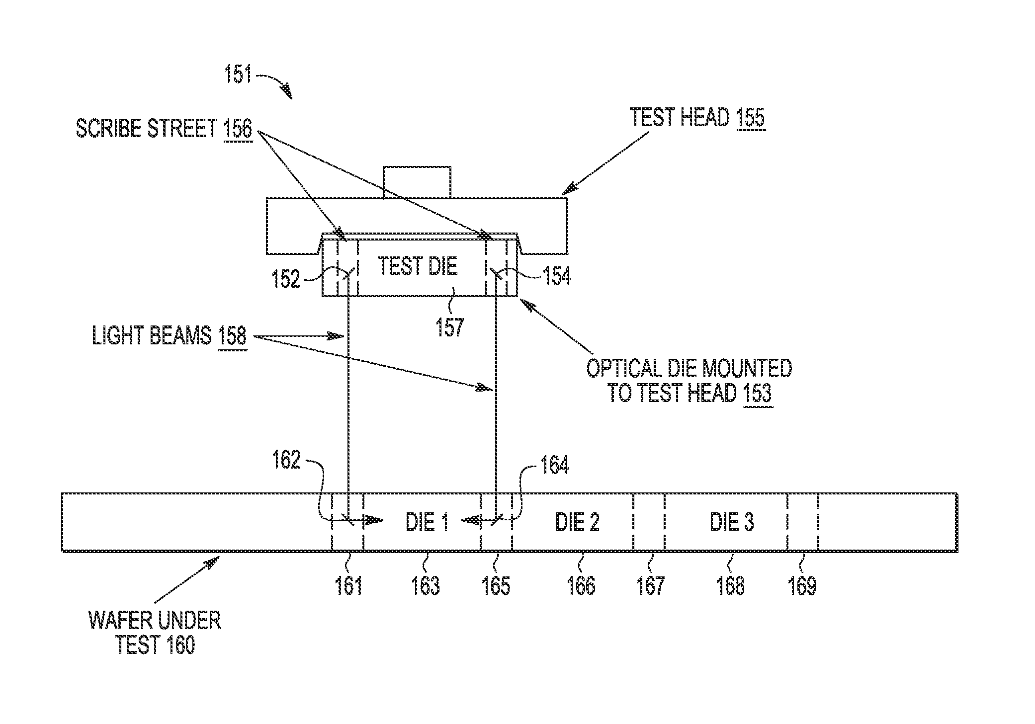
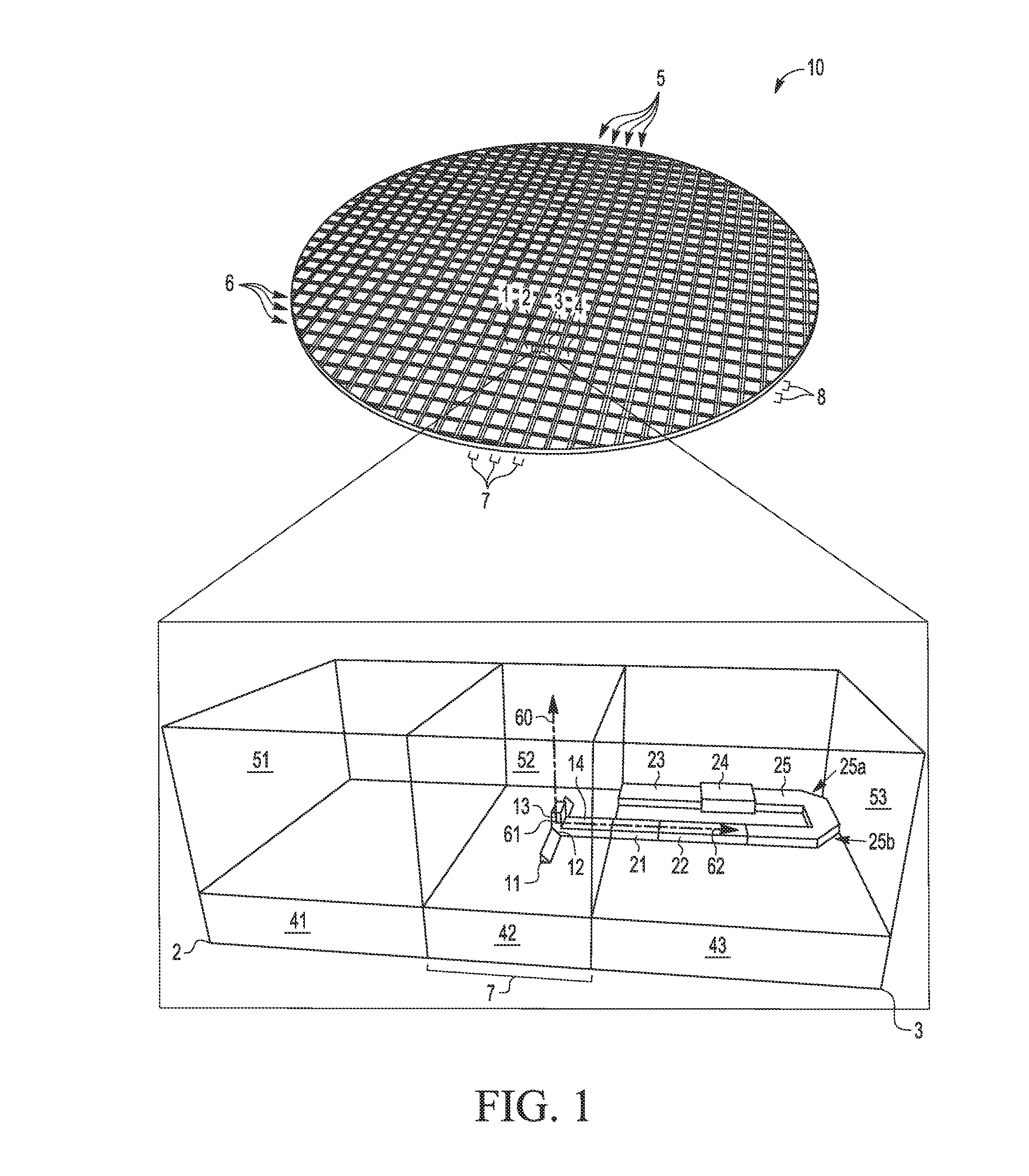
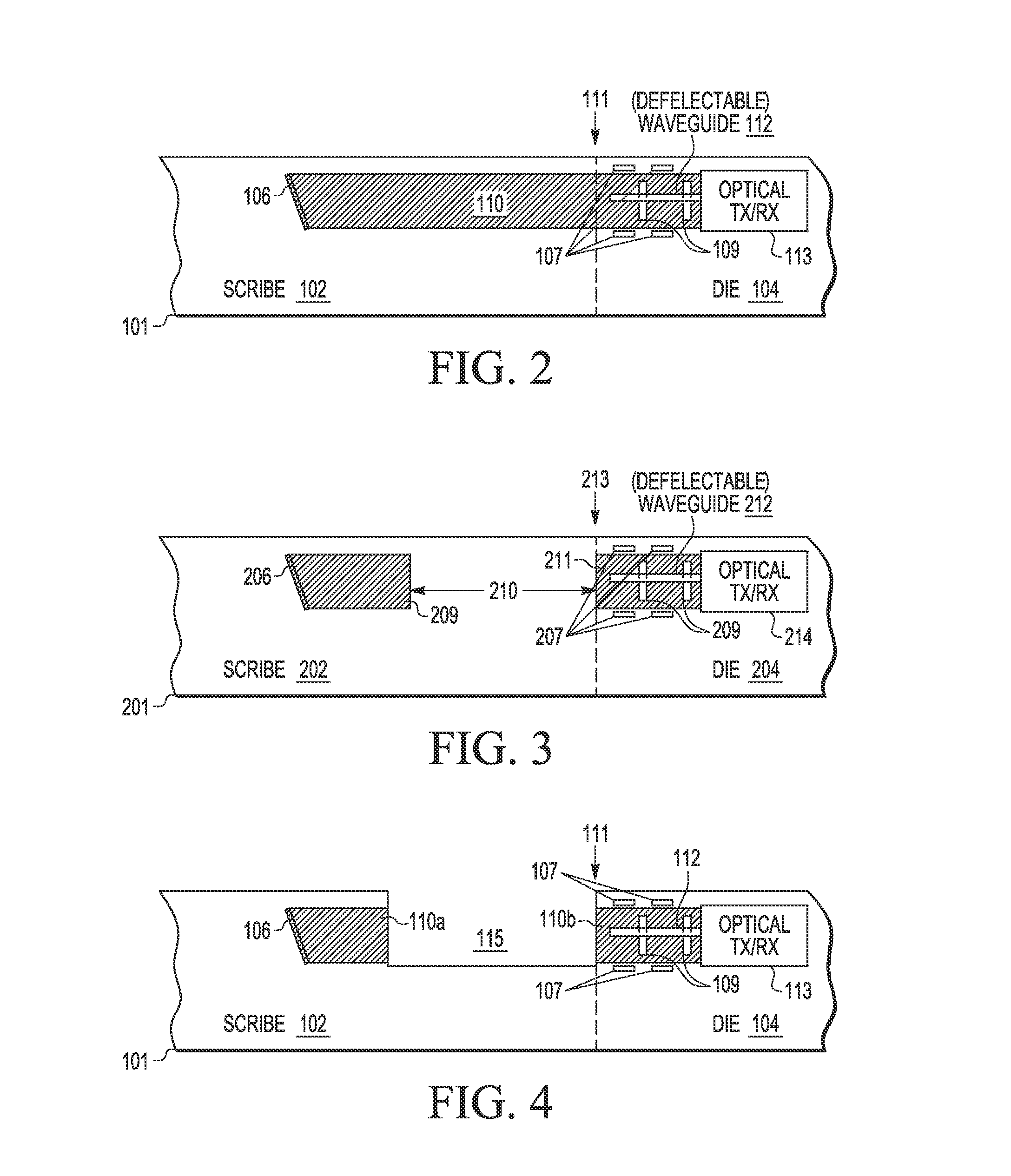
[0020]There is disclosed herein an improved optical die test interface and associated die probe test arrangement and methodology, for testing high density, low power, high performance optical communication systems in integrated circuit devices that address various problems in the art where various limitations and disadvantages of conventional solutions and technologies will become apparent to one of skill in the art after reviewing the remainder of the present application with reference to the drawings and detailed description provided herein. In selected embodiments, a system, method and apparatus are described for fabricating one or more mirror structures (e.g., 45 degree mirrors) in the scribe areas around each die on a wafer to perform wafer level tests of optical and composite die. By using silicon orientation-dependent wet etch processes to perform silicon micromachining, 45 degree mirror structures may be fabricated in the scribe street or grid area to perpendicularly deflect...


PUM


Abstract

An optical die probe wafer testing circuit arrangement and associated testing methodology are described for mounting a production test die (157) and surrounding scribe grid (156) to a test head (155) which is positioned over a wafer (160) in alignment with a die under test (163) and surrounding scribe grid (161, 165), such that one or more optical deflection mirrors (152, 154) in the test head scribe grid (156) are aligned with one or more optical deflection mirrors (162, 164) in the scribe grid (161, 165) for the die under test (163) to enable optical die probe testing on the die under test (163) by directing a first optical test signal (158) from the production test die (157), through the first and second optical deflection mirrors (e.g., 152, 162) and to the first die.

Description

CROSS-REFERENCE TO RELATED APPLICATIONS[0001]U.S. Pat. No. ______, entitled “Die Stack with Optical TSVS,” by inventors Perry H. Pelley, Tab A. Stephens, and Michael B. McShane, Attorney Docket No. DN30660TK, filed on even date herewith, describes exemplary methods and systems and is incorporated by reference in its entirety.[0002]U.S. Pat. No. ______, entitled “Communication System Die Stack,” by inventors Tab A. Stephens, Perry H. Pelley, and Michael B. McShane, Attorney Docket No. FS40406TK, filed on even date herewith, describes exemplary methods and systems and is incorporated by reference in its entirety.[0003]U.S. Pat. No. ______, entitled “Integration of a MEMS Beam with Optical Waveguide and Deflection in Two Dimensions,” by inventors Tab A. Stephens, Perry H. Pelley, and Michael B. McShane, Attorney Docket No. FS40407ZR, filed on even date herewith, describes exemplary methods and systems and is incorporated by reference in its entirety.[0004]U.S. Pat. No. ______, entitled...

Claims


Application Information

Patent Timeline
Patent Type & Authority Applications(United States)
IPC IPC(8): G01R31/27H01L21/78H01L31/18H01L21/66
CPCG01R31/275H01L31/18H01L22/10H01L21/78G01R31/2886H01L22/12G02B6/42G02B6/30G01R31/2889G01M11/00
Inventor MCSHANE, MICHAEL B.PELLEY, PERRY H.STEPHENS, TAB A.
Owner NXP USA INC
Why Eureka
Try Eureka