Wafer-level opto-electronic testing apparatus and method

a technology of optoelectronic and wafer-level, applied in the direction of individual semiconductor device testing, semiconductor/solid-state device testing/measurement, instruments, etc., can solve the problems of severe limitation of circuits, destructive testing of arrangement, waste of valuable time and money, etc., to enhance optical coupling efficiency and enhance coupling efficiency

Active Publication Date: 2006-09-19
CISCO TECH INC
View PDF12 Cites 28 Cited by
  • Summary
  • Abstract
  • Description
  • Claims
  • Application Information

AI Technical Summary

Benefits of technology

[0011]The input and output optical test signals may be coupled using an array of optical fibers, preferably polarization maintaining fibers. Exterior lenses (or integral lenses formed on the fiber endface) may be used to enhance optical coupling efficiency. Input wavelength tuning may be performed to match the mode angle of the waveguide being tested on the wafer surface and thus enhance coupling efficiency, utilizing one or more feedback signals from the wafer to control the tuning.

Problems solved by technology

If the performance of the individual circuits is not tested prior to dicing, a “bad” chip may be further processed and packaged, wasting valuable time and money.
The need to have access to the “edges” of the circuit is considered to be a severe limitation of this particular wafer-level optical testing method.
While this arrangement eliminates the need to perform “edge” contacts, this type arrangement is considered as “destructive testing”, since a portion of the circuit must be removed to perform the testing.
Obviously, when performing repeated tests at multiple circuit locations on a wafer, destructive testing is not a preferred choice.
Moreover, both of these prior art arrangements require the use of index matching fluids between the optical probe and the wafer (raising issues regarding reproducibility of measurements and contamination) and provide only optical testing; a traditional electronic “probe card” is still required to analyze and test the electronics on the wafer.

Method used


Image

  • Wafer-level opto-electronic testing apparatus and method
  • Wafer-level opto-electronic testing apparatus and method
  • Wafer-level opto-electronic testing apparatus and method

Examples


Embodiment Construction

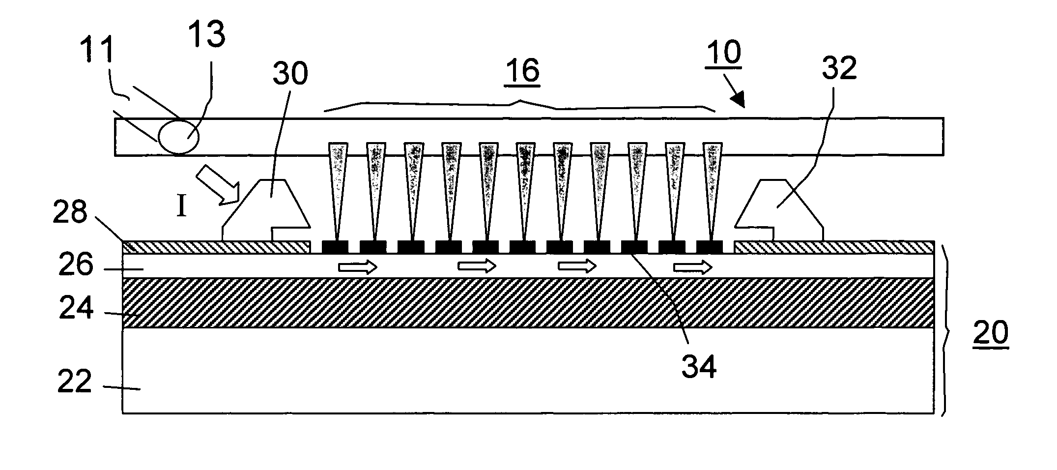
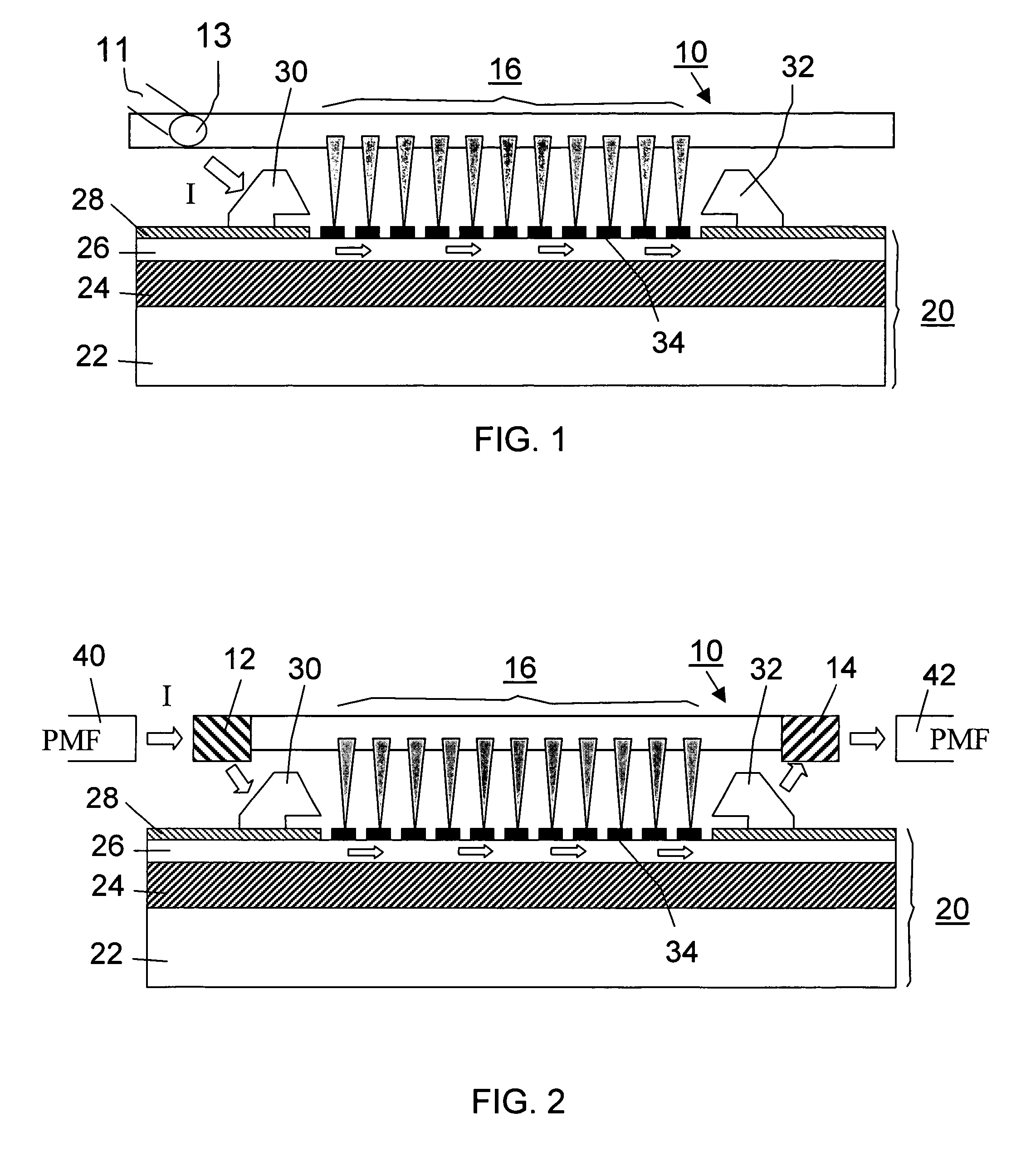
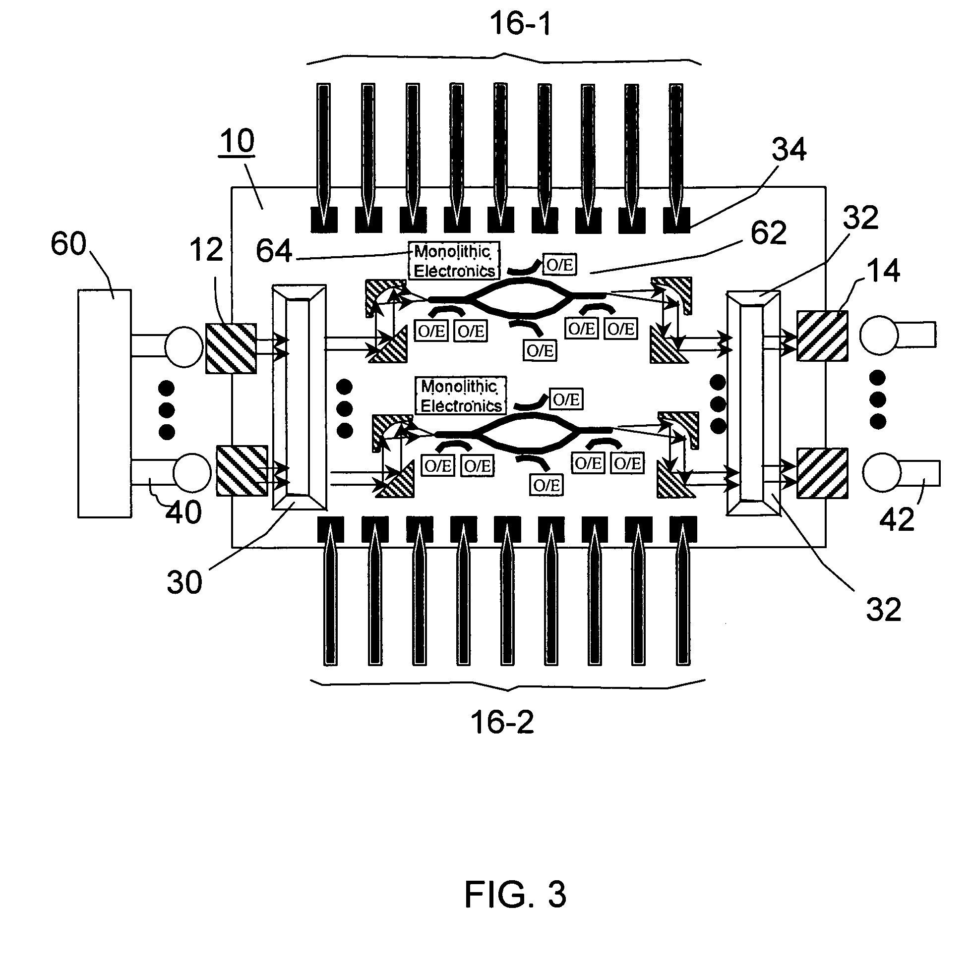
[0019]As briefly alluded to above, one of the biggest challenges in the development of an optical testing element for SOI-based optical structures is the need to reliably couple an optical beam into a very thin waveguide being tested in a repeatable fashion. The angle at which the light is required to enter the thin waveguide is known to be a strong function of the waveguide thickness and the wavelength of the optical signal (that is, the mode angle of the light entering the SOI structure needs to be well-controlled so as to excite a specific mode in the waveguide). An aspect of the present invention is the ability to “tune” the wavelength of the test signal over a range such that acceptable coupling can be reliably achieved on a repeatable basis. Inasmuch as process variations will alter the thickness of the waveguiding layer from wafer to wafer, as well as the thickness of the associated evanescent coupling layer, the ability to monitor and “tune” the test wavelength in accordance...


PUM


Abstract

A wafer-level testing arrangement for opto-electronic devices formed in a silicon-on-insulator (SOI) wafer structure utilizes a single opto-electronic testing element to perform both optical and electrical testing. Beam steering optics may be formed on the testing element and used to facilitate the coupling between optical probe signals and optical coupling elements (e.g., prism couplers, gratings) formed on the top surface of the SOI structure. The optical test signals are thereafter directed into optical waveguides formed in the top layer of the SOI structure. The opto-electronic testing element also comprises a plurality of electrical test pins that are positioned to contact a plurality of bondpad test sites on the opto-electronic device and perform electrical testing operations. The optical test signal results may be converted into electrical representations within the SOI structure and thus returned to the testing element as electrical signals.

Description

CROSS-REFERENCE TO RELATED APPLICATION[0001]This application claims the benefit of U.S. Provisional Application No. 60 / 551,316, filed Mar. 8, 2004.TECHNICAL FIELD[0002]The present invention relates to the provisioning of wafer-level testing and, more particularly, to the capability of providing optical, electrical and opto-electronic testing of various elements formed on a silicon-on-insulator (SOI) structure using a single testing element.BACKGROUND OF THE INVENTION[0003]In the semiconductor industry, a relatively large silicon wafer (generally on the order of several inches in diameter) is processed to form a multiple number of identical integrated circuits. Once the wafer has been completely processed, it is “diced” apart to form the individual integrated circuits. In most cases, hundreds of identical circuits are formed across the wafer surface. If the performance of the individual circuits is not tested prior to dicing, a “bad” chip may be further processed and packaged, wastin...

Claims


Application Information

Patent Timeline
Patent Type & Authority Patents(United States)
IPC IPC(8): G01R31/26G01R31/00
CPCG02B6/30G02B6/34G02B2006/12107H01L22/00
Inventor GOTHOSKAR, PRAKASHGHIRON, MARGARETMONTGOMERY, ROBERT KEITHPATEL, VIPULKUMARSHASTRI, KALPENDUPATHAK, SOHAMPIEDE, DAVIDYANUSHEFSKI, KATHERINE A.
Owner CISCO TECH INC
Why Eureka
Try Eureka