MEMS structure and method of forming the same

a technology of microelectromechanical systems and meshes, applied in the field of mesh structure, can solve problems such as damage during etching, and achieve the effect of preventing the risk of improving process window or performance, and preventing damage to the mesh structur

Active Publication Date: 2014-12-18
UNITED MICROELECTRONICS CORP
View PDF6 Cites 9 Cited by
  • Summary
  • Abstract
  • Description
  • Claims
  • Application Information

AI Technical Summary

Benefits of technology

[0006]One objective of the present invention is to provide a method of forming a MEMS structure, and in which a MEMS component, such as MEMS diaphragm, will be not damaged during an etch process for forming an opening from backside of the substrate.
[0009]In the method according to the present invention, an etch stop layer is formed to be buried within the inter-dielectric layer, such that when the substrate and the inter-dielectric layer are etched in order to form a chamber, the etch is allowed to stop at the etch stop layer. Accordingly, the MEMS structure is prevented from the risk of being damaged by etching, and a process window or performance can be improved.

Problems solved by technology

However, the MEMS diaphragm is directly used as an oxide etch stop without using other extra etch stop layer and may be damaged during the etch.

Method used


Image

  • MEMS structure and method of forming the same
  • MEMS structure and method of forming the same
  • MEMS structure and method of forming the same

Examples


Embodiment Construction

[0016]Some embodiments or modifications according to the present invention will be further described hereinafter. For conciseness and easy comparison among the embodiments or modifications, the same elements will be denoted with the same referral numbers or symbols, and the same contents may be not described again.

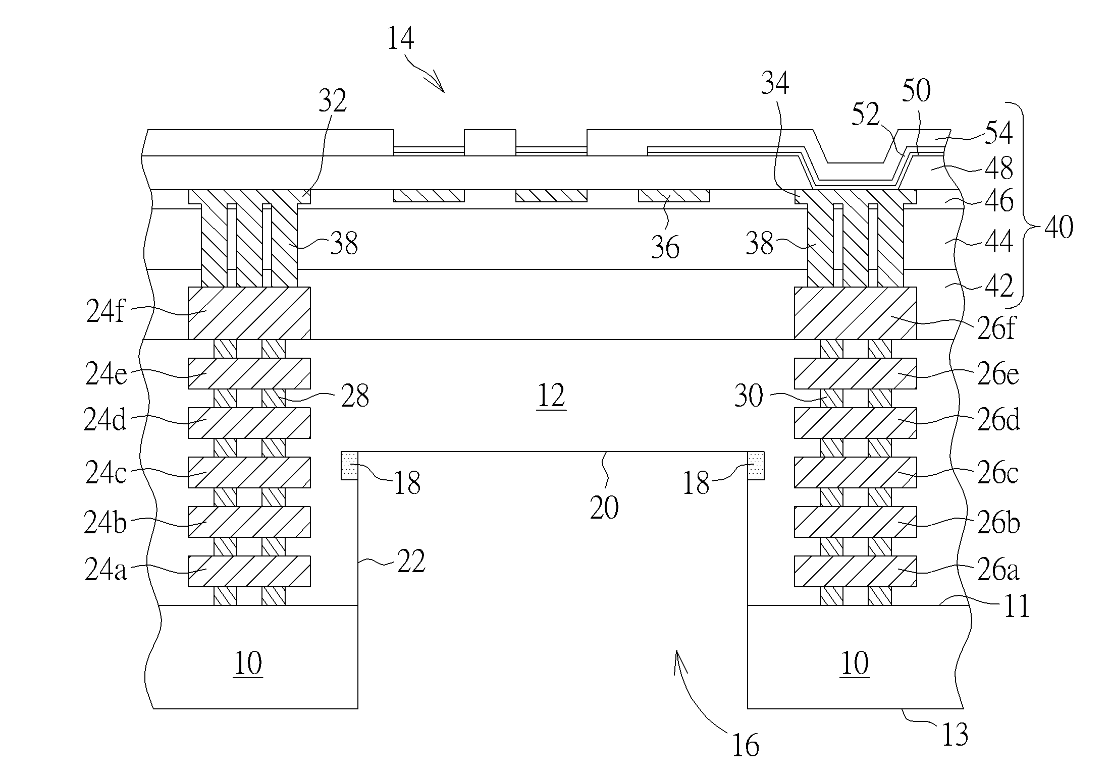
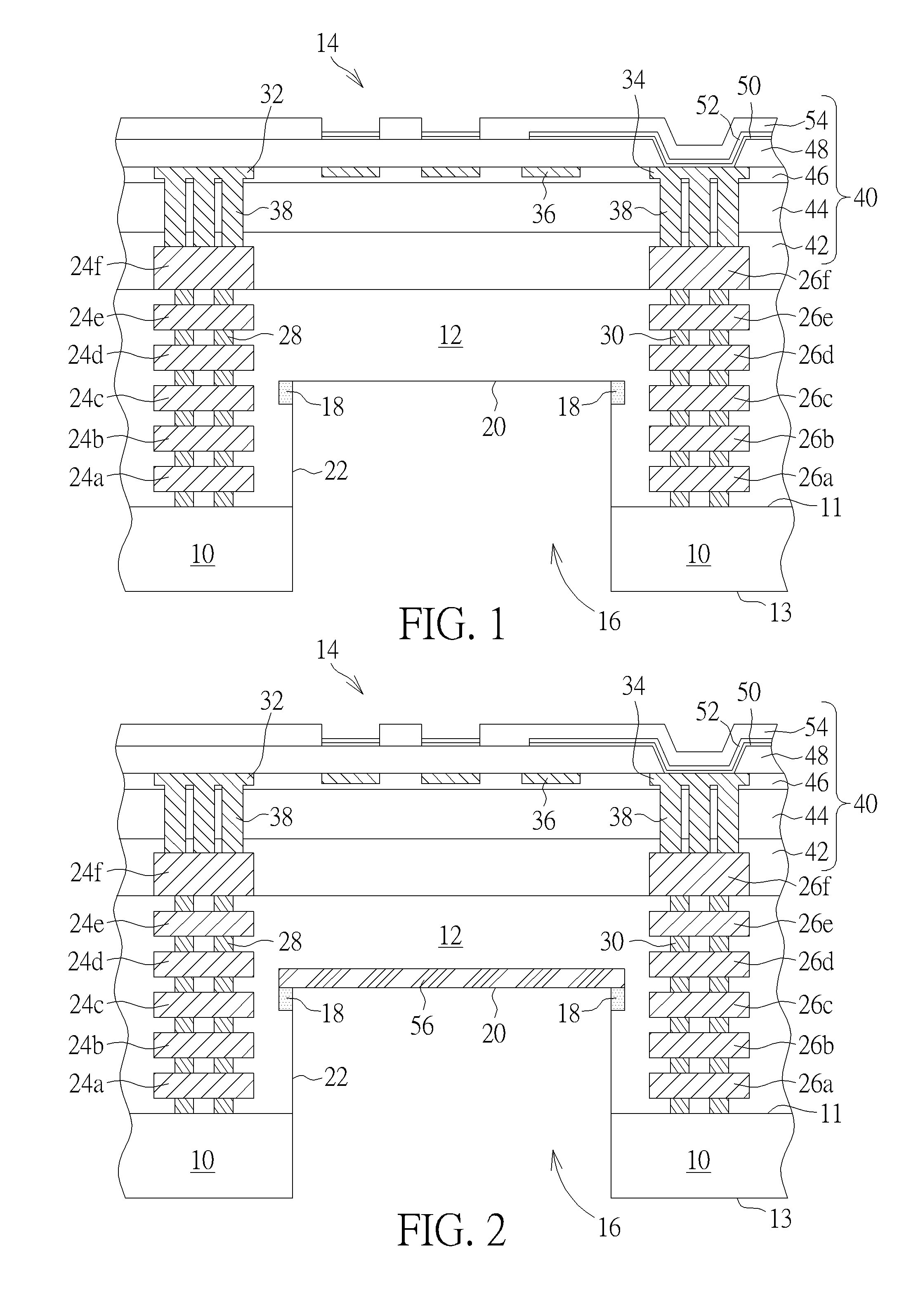
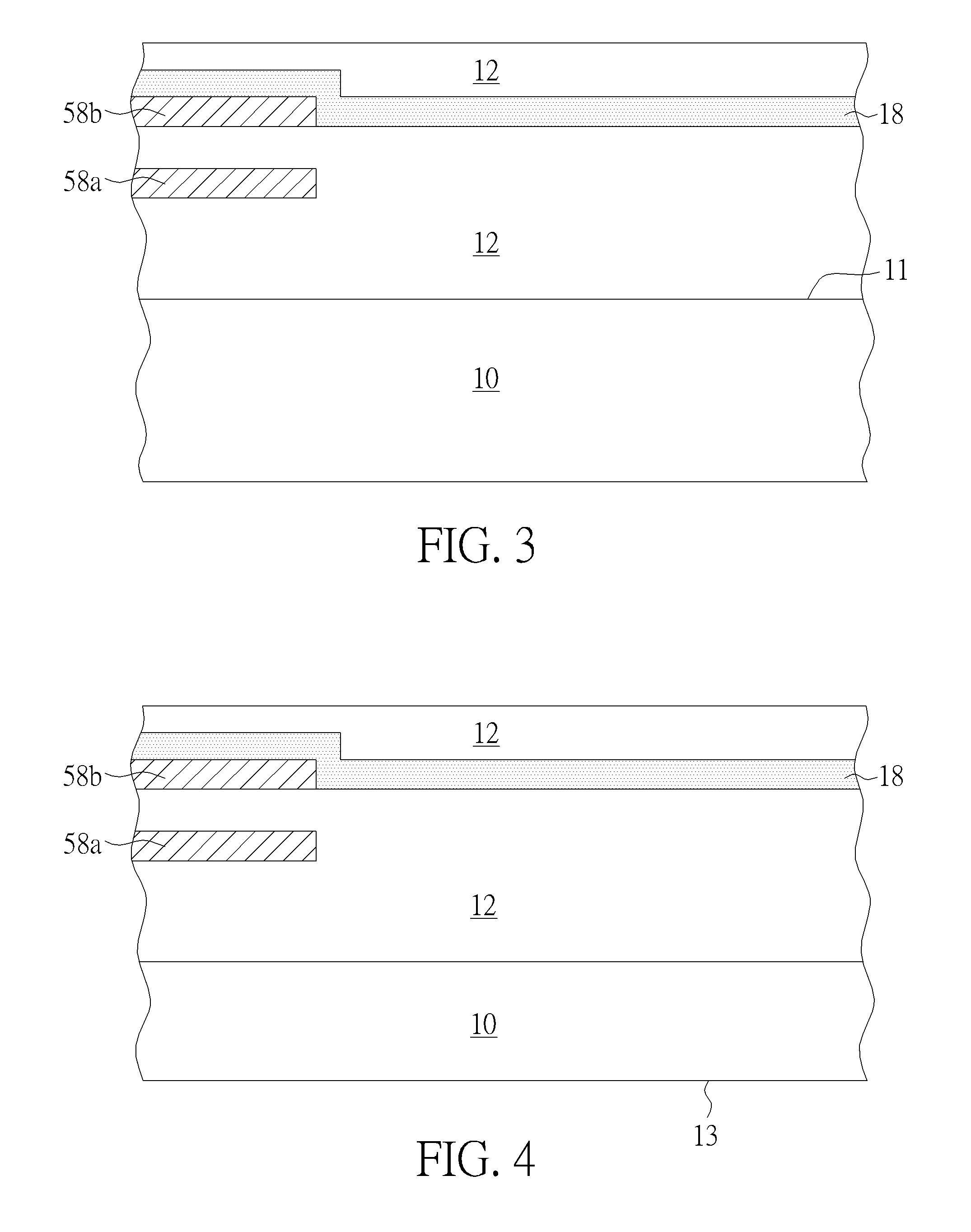
[0017]Referring to FIG. 1, a MEMS structure according to a first embodiment of the present invention includes a substrate 10, an inter-dielectric layer 12 on a front side 11 of the substrate 10, a MEMS component 14 on the inter-dielectric layer 12, and a chamber 16 disposed within the inter-dielectric layer 12 and through the substrate 10. The inter-dielectric layer 12 represents a collection of all dielectric layers between the substrate 10 and the MEMS component 14. A certain thickness of inter-dielectric layer 12 remains between the MEMS component 14 and the chamber 16. The chamber 16 has an opening at a backside 13 of the substrate 10. An etch stop layer 18 is disposed...


PUM

PropertyMeasurementUnit
thicknessaaaaaaaaaa
thicknessaaaaaaaaaa
thicknessaaaaaaaaaa

Abstract

A method of forming a MEMS structure, in which an etch stop layer is formed to be buried within the inter-dielectric layer and, during an etch of the substrate and the inter-dielectric layer from backside to form a chamber, the etch stop layer protect the remaining inter-dielectric layer. The chamber thus formed has an opening at a backside of the substrate, a ceiling opposite to the opening, and a sidewall joining the ceiling. The sidewall may further include a portion of the etch stop layer.

Description

BACKGROUND OF THE INVENTION[0001]1. Field of the Invention[0002]The present invention relates to a microelectromechanical system (MEMS) technology, and particularly relates to a MEMS structure and a method of fabricating such MEMS structure.[0003]2. Description of the Prior Art[0004]MEMS devices can be applied in many applications, such as accelerometer, gyro sensor, flow meter, microphone, microspeaker, and so on, and serves as microsensors, microactuators, and so on, operating based on, for example, electromagnetic, electrostrictive, thermoelectric, piezoelectric, or piezoresistive effects. It is preferred that the method for making an MEMS device is compatible with a standard CMOS manufacturing process.[0005]Currently, a MEMS pressure sensing device is made in the way to allow the substrate to have an opening from backside and form a chamber on the inter-dielectric layers by dry or wet etch process. However, the MEMS diaphragm is directly used as an oxide etch stop without using ...

Claims


Application Information

Patent Timeline
Patent Type & Authority Applications(United States)
IPC IPC(8): B81C1/00
CPCB81C1/00801B81C2201/014B81C2203/0714B81C1/00246B81C2203/0735B81C1/00587B81C1/00555B81C1/00595B81C1/00563B81B2201/0264B81B2203/0127B81B3/0075B81B2207/07
Inventor CHEN, LI-CHEWU, TE-YUANLIN, CHIA-HUEIWU, HUI-MINHSIEH, KUN-CHEWANG, KUAN-YUCHIU, CHUNG-YI
Owner UNITED MICROELECTRONICS CORP
Why Eureka
Try Eureka