
Digital domain accumulative cmos-tdi image sensor with low power consumption

Active Publication Date: 2014-12-18
QUANTRON
View PDF5 Cites 17 Cited by
  • Summary
  • Abstract
  • Description
  • Claims
  • Application Information

AI Technical Summary

Benefits of technology

The present invention provides a digital domain accumulative CMOS-TDI image sensor with low power consumption. It includes a pixel array, a column parallel signal pre-processing circuit, a column parallel successive approximation (SAR)ADC, a column parallel digital domain accumulator, a column parallel divider, a timing control circuit and an output shift register. The sensor reduces power consumption by reducing the conversion rate of the SARADC without reducing the line frequency of the CMOS-TDI image sensor. To achieve this, the sensor includes a pixel array with an increased number of rows and columns, a column parallel signal pre-processing circuit, a column parallel SARADC, a column parallel digital domain accumulator, a column parallel divider and a timing control circuit. The sensor also includes a column parallel coarse quantification memory unit and a column parallel fine quantification memory unit to perform multiple stages of TDI signal accumulation. This results in a sensor with reduced power consumption and improved image quality.

Problems solved by technology

However, as the object is moving continuously during pixel exposure of the linear array image sensor, the pixel exposure period is seriously limited by the moving speed of the sensor relative to the object being shot.
CCD image sensors presently used in many technical fields however, have been gradually replaced by CMOS (Complementary Metal Oxide Semiconductor) image sensors due to disadvantages such as large power consumption and low integration.
This method of realizing CMOS-TDI image sensor by accumulation of analog signals however will consume much power and result in large chip size.
In addition, great noise may also be introduced by the analog signal accumulator itself during accumulation of analog signals, thus leading to much difficulty in forming higher TDI stage.
Therefore, it is very difficult to reduce power consumption of the CMOS-TDI image sensor when realizing high line frequency.

Method used


Image

  • Digital domain accumulative cmos-tdi image sensor with low power consumption
  • Digital domain accumulative cmos-tdi image sensor with low power consumption
  • Digital domain accumulative cmos-tdi image sensor with low power consumption

Examples


Embodiment Construction

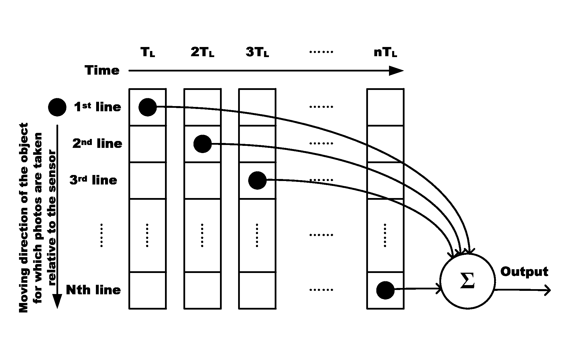
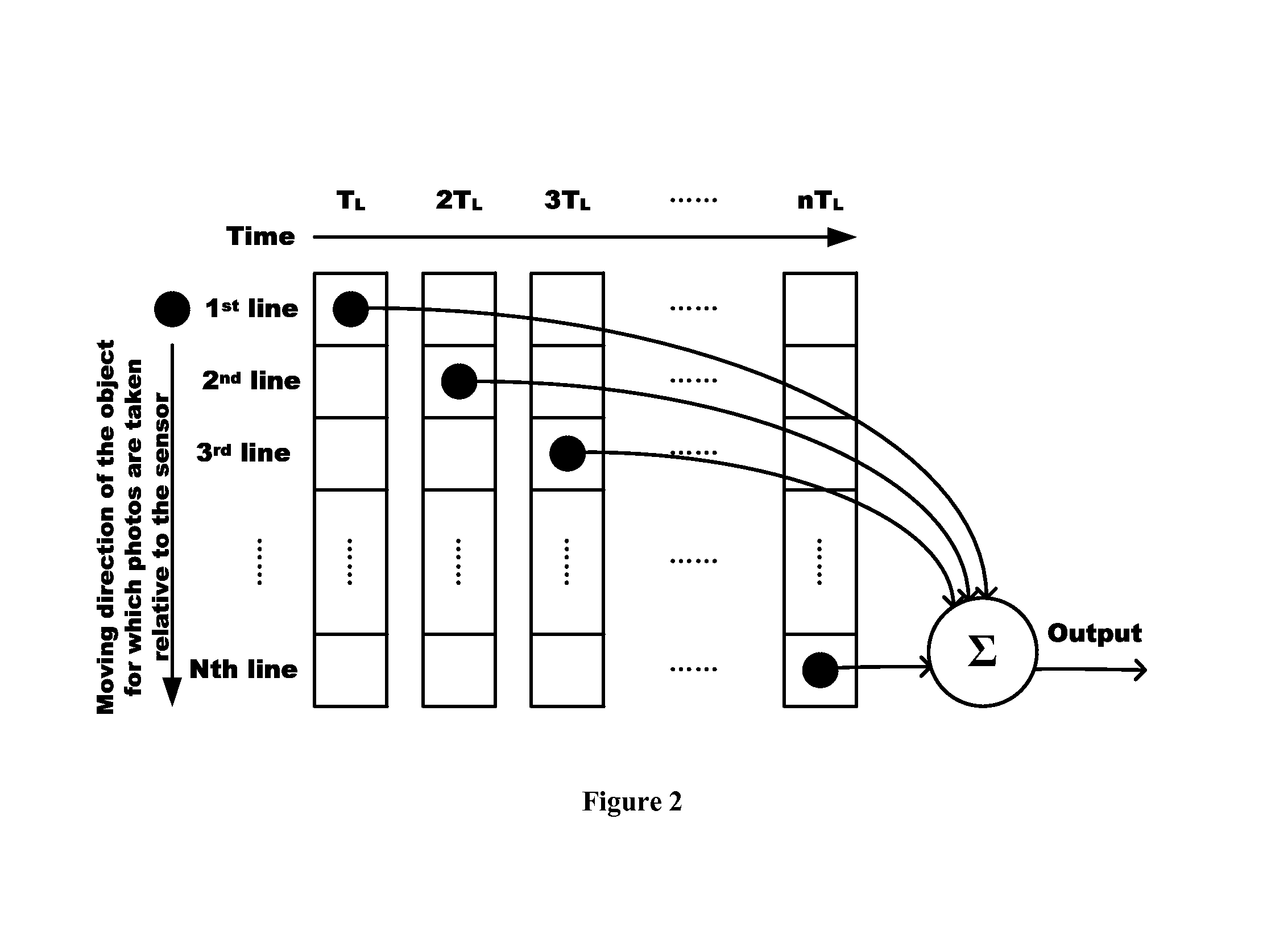
[0015]K lines of pre-processing pixels (P1−Pk) are added into an n×m pixel array (n lines and m columns). The newly added k lines of pre-processing pixels are located to face a direction along which the original pixel array moves towards the object. The detailed construction of the sensor is shown in FIG. 3. The digital domain accumulative CMOS-TDI image sensor mainly includes a pixel array of (n+k)×m ((n+k) lines and m columns), a column parallel signal pre-processing circuit (CDS and signal amplification), a column parallel SAR ADC (successive approximation ADC), a column parallel digital domain accumulator, a column parallel divider, a timing control circuit and an output shift register. In the prior art, attempt has been made in order to achieve that the CMOS-TDI will perform exposure to the same object synchronously by temporal over-sampling method. The rolling shutter exposure with over-sampling rate of (n+k+1) / (n+k) has also been applied to the digital domain accumulative CMO...


PUM


Abstract

The present invention relates to the field of design of analog digital hybrid integrated circuit. The object of the invention is to reduce ADC conversion rate thus further reducing power consumption of the sensor while not reducing line frequency of the CMOS-TDI. To this end, a digital domain accumulative CMOS-TDI image sensor with low power consumption is provided. It includes a pixel array of n+k lines multiplied m columns, a column parallel signal pre-processing circuit, a column parallel successive approximation (SAR) ADC, a column parallel digital domain accumulator, a column parallel divider, a timing control circuit and an output shift register, wherein n+k+1 coarse quantification memory units are provided to the column parallel digital domain accumulator for storage of coarse quantification results; and memory units for storage of n times of fine quantification results are also provided, thus realizing n stages of TDI signal accumulation after accumulation of n times of fine quantification results. The invention is generally used in hybrid integrated circuit design.

Description

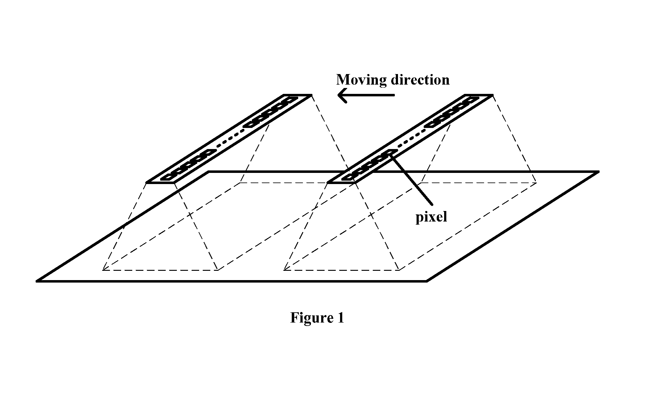
FIELD OF THE INVENTION[0001]The present invention relates to the field of design of analog digital hybrid integrated circuit and more particularly, relates to a method of decreasing power consumption of digital domain accumulative CMOS-TDI image sensors and further relates to a digital domain accumulative CMOS-TDI image sensor with low power consumption.BACKGROUND OF THE INVENTION[0002]An image sensor is capable of transforming optical signals captured by lens into electrical signals which may be easily stored, transferred and processed. The image sensor can be classified into area array type and linear array based on working principle. The area array image sensor works under the following principle: photos of an object are taken by a two-dimensional pixel array so as to obtain two-dimensional image information. The linear array image sensor works under the following principle: photos of an object are taken by scanning action of a single-dimensional pixel array to obtain two-dimensi...

Claims


Application Information

Patent Timeline
IPC IPC(8): H04N5/3745H04N5/378H04N5/374
CPCH04N5/37455H04N5/378H04N5/3743H04N25/768H04N25/75H04N25/772
Inventor YAO, SUYINGNIE, KAIMINGXU, JIANGTAOGAO, JINGSHI, ZAIFENGGAO, CEN
Owner QUANTRON
Learn More