Imaging device

a technology of imaging device and detector, which is applied in the direction of radiation control device, semiconductor device, electrical apparatus, etc., can solve the problems of degrading the reliability or increasing power consumption of the flat panel detector, and achieves high resolution, low power consumption, and high stability to irradiation.

Active Publication Date: 2014-12-25
SEMICON ENERGY LAB CO LTD
View PDF4 Cites 9 Cited by
  • Summary
  • Abstract
  • Description
  • Claims
  • Application Information

AI Technical Summary

Benefits of technology

[0013]Thus, an object of one embodiment of the present invention is to provide an imaging device that is highly stable to irradiation with radial rays such as X-rays. Another object of one embodiment of the present invention is to provide an imaging device having a structure that can inhibit a decrease in electrical characteristics. Another object of one embodiment of the present invention is to provide an imaging device with high resolution. Another object of one embodiment of the present invention is to provide an imaging device capable of taking an image with low dose of radiation. Another object of one embodiment of the present invention is to provide an imaging device with low power consumption. Another object of one embodiment of the present invention is to provide an imaging device with high reliability. Another object of one embodiment of the present invention is to provide a novel imaging device or the like.
[0021]With one embodiment of the present invention, an imaging device that is highly stable to irradiation with radial rays such as X-rays can be provided. An imaging device having a structure that can inhibit a decrease in electrical characteristics can be provided. An imaging device with high resolution can be provided. An imaging device capable of taking an image with low dose of radiation can be provided. An imaging device with low power consumption can be provided. An imaging device with high reliability can be provided. A novel imaging device or the like can be provided.

Problems solved by technology

This phenomenon can occur by a slight amount of radial rays that have penetrated a scintillator, which is one cause for increasing power consumption or degrading reliability of the flat panel detector.

Method used


Image

  • Imaging device
  • Imaging device
  • Imaging device

Examples


embodiment 1

[0051]In this embodiment, an imaging device using radial rays such as X-rays, which is one embodiment of the present invention, is described with reference to the drawings.

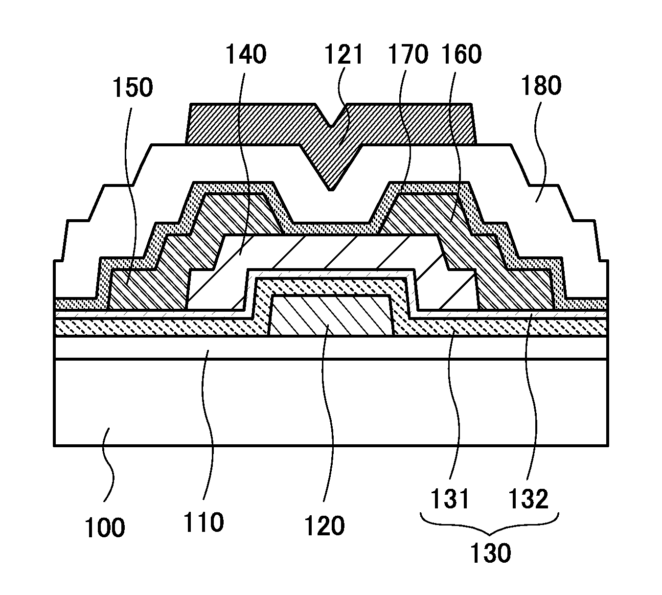
[0052]FIG. 1 is a cross-sectional view of a transistor that can be used in an imaging device using radial rays such as X-rays, which is one embodiment of the present invention. The transistor includes a base insulating film 110 over a substrate 100, a gate electrode layer 120 over the base insulating film 110, a gate insulating film 130 including a first insulating film 131 and a second insulating film 132 in this order over the gate electrode layer, an oxide semiconductor layer 140 over the gate insulating film, and a source electrode layer 150 and a drain electrode layer 160 which are each in contact with part of the oxide semiconductor layer. An insulating layer 170 may be formed over the gate insulating film 130, the oxide semiconductor layer 140, the source electrode layer 150, and the drain electrode layer 1...

embodiment 2

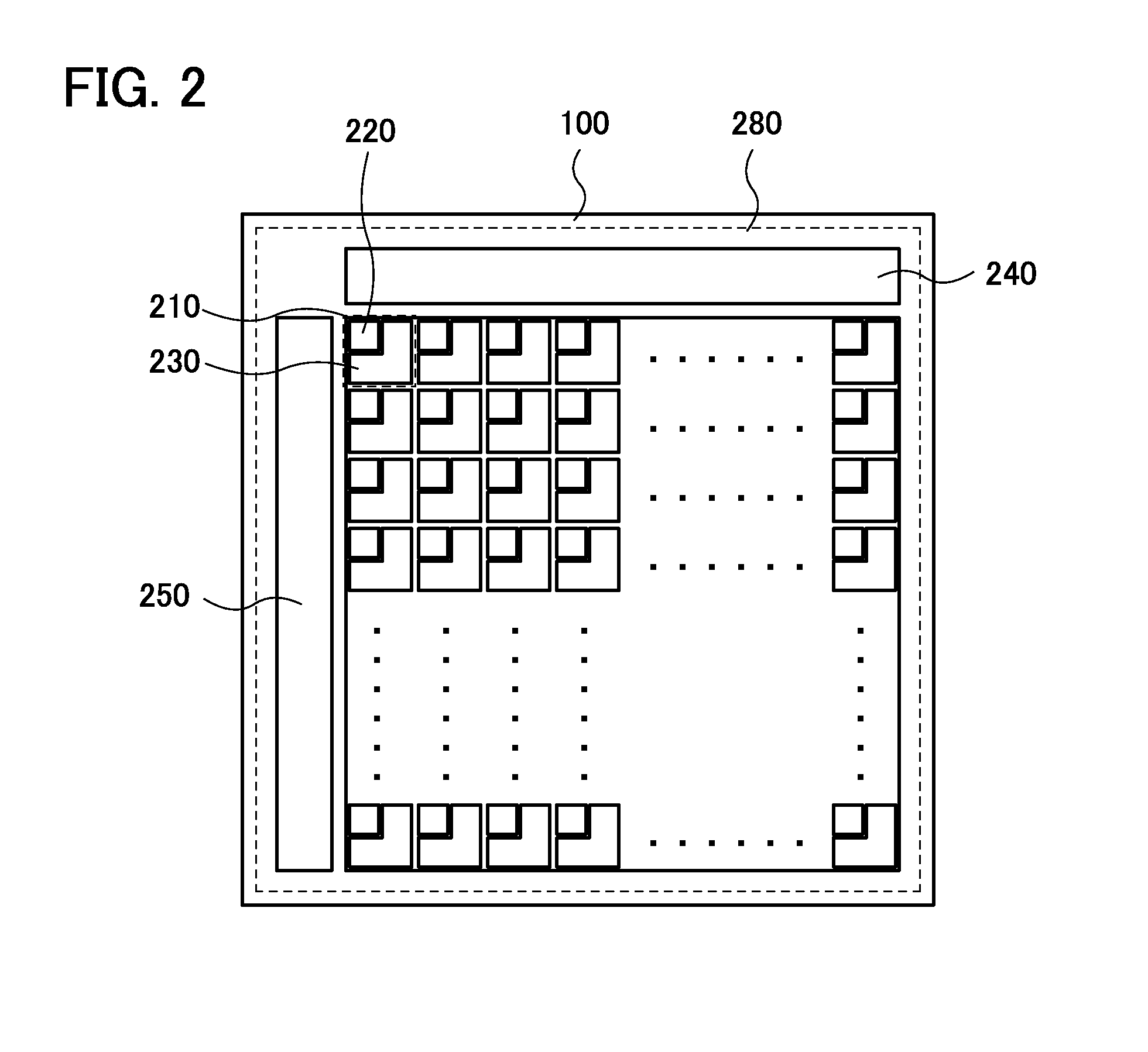
[0076]In this embodiment, a pixel circuit that can use the transistor described in Embodiment 1 will be described.

[0077]FIG. 5A shows an example of a circuit that can be used as the pixel circuit 210 illustrated in FIG. 2. A circuit 211 includes a photodiode 320 serving as the light-receiving element 220 and a first transistor 301, a second transistor 302, and a third transistor 303 that are provided in the circuit portion 230 connected to the light-receiving element.

[0078]An anode of the photodiode 320 is electrically connected to a first wiring 311 (RS); a cathode of the photodiode 320 is electrically connected to one of a source and a drain of the first transistor 301; the other of the source and the drain of the first transistor 301 is electrically connected to a wiring 305 (FD); a gate of the first transistor 301 is electrically connected to a second wiring 312 (TX); one of a source and a drain of the second transistor 302 is electrically connected to a fourth wiring 314 (GND);...

embodiment 3

[0132]In this embodiment, an example of a driving method of the pixel circuit described in Embodiment 2 is described.

[0133]As described in Embodiment 2, the operation of the pixel circuit is repetition of the reset operation, the accumulation operation, and the selection operation. In the imaging device using radial rays such as X-rays, radiation exposure time is preferably as short as possible in consideration of influence of radial rays on the living body. To shorten the radiation irradiation time and perform imaging in short time, it is necessary to perform the reset operation, the accumulation operation, and the selection operation of all the pixel circuits at high speed.

[0134]Thus, a driving method using a global shutter system illustrated in a timing chart in FIG. 11A is preferably used for imaging. Note that FIG. 11A shows operations of the imaging device in which a plurality of pixel circuits 211 illustrated in FIG. 5A are arranged in a matrix, specifically, operations of th...


PUM


Abstract

An imaging device that is highly stable to irradiation with radial rays such as X-rays and can inhibit a decrease in electrical characteristics is provided. The imaging device takes an image with radial rays such as X-rays and includes pixel circuits arranged in a matrix and a scintillator overlapping the pixel circuits. The pixel circuits each includes a switching transistor with an extremely small off-state current and a light-receiving element which is configured to convert the radial rays to electrical charges. A gate insulating film of the switching transistor has a stacked structure including a silicon nitride film with a thickness of 100 nm to 400 nm and a silicon oxide film or a silicon oxynitride film with a thickness of 5 nm to 20 nm.

Description

BACKGROUND OF THE INVENTION[0001]1. Field of the Invention[0002]One embodiment of the present invention relates to an imaging device.[0003]Note that one embodiment of the present invention is not limited to the above technical field. The technical field of one embodiment of the invention disclosed in this specification and the like relates to an object, a method, or a manufacturing method. In addition, one embodiment of the present invention relates to a process, a machine, manufacture, or a composition of matter. Specifically, examples of the technical field of one embodiment of the present invention disclosed in this specification include a semiconductor device, a display device, a liquid crystal display device, a light-emitting device, a lighting device, a power storage device, a storage device, an imaging device, a method for driving any of them, and a method for manufacturing any of them.[0004]In this specification and the like, a semiconductor device means a general device tha...

Claims


Application Information

Patent Timeline
Patent Type & Authority Applications(United States)
IPC IPC(8): H01L27/146H01L29/786
CPCH01L27/14663H01L27/14659H01L29/7869H01L27/14625H01L27/14616H01L29/42384H01L29/4908H01L27/14692H04N25/77H01L29/78606H01L29/78651
Inventor TAKAHASHI, HIRONOBUSHIMA, YUKINORIHOSAKA, YASUHARUOBONAI, TOSHIMITSUTSUBUKU, MASASHI
Owner SEMICON ENERGY LAB CO LTD
Why Eureka
Try Eureka