Ceramic electronic component and method of manufacturing the same

a technology of ceramic electronic components and manufacturing methods, applied in the direction of fixed capacitors, magnets, magnetic bodies, etc., can solve the problems of high hygroscopicity of resin, increased water vapor generated during heating, and increased so as to reduce the probability of solder burst or prevent the effect of occurren

Active Publication Date: 2014-12-25
MURATA MFG CO LTD
View PDF10 Cites 18 Cited by
  • Summary
  • Abstract
  • Description
  • Claims
  • Application Information

AI Technical Summary

Benefits of technology

[0014]Preferred embodiments of the present invention provide a ceramic electronic component and a method of manufacturing the same, which significantly reduce or prevent the occurrence of solder burst.
[0024]According to various preferred embodiments of the present invention, the occurrence of solder burst is significantly reduced or prevented.

Problems solved by technology

In general, a resin is high in hygroscopicity and tends to absorb moisture.
Then, an amount of water vapor generated during heating increases, and solder burst is more likely.

Method used


Image

  • Ceramic electronic component and method of manufacturing the same
  • Ceramic electronic component and method of manufacturing the same
  • Ceramic electronic component and method of manufacturing the same

Examples


Embodiment Construction

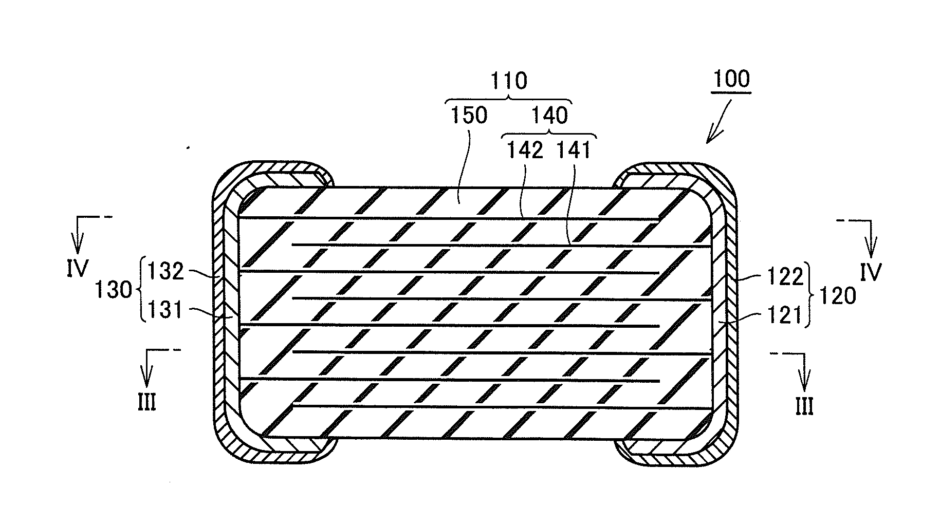
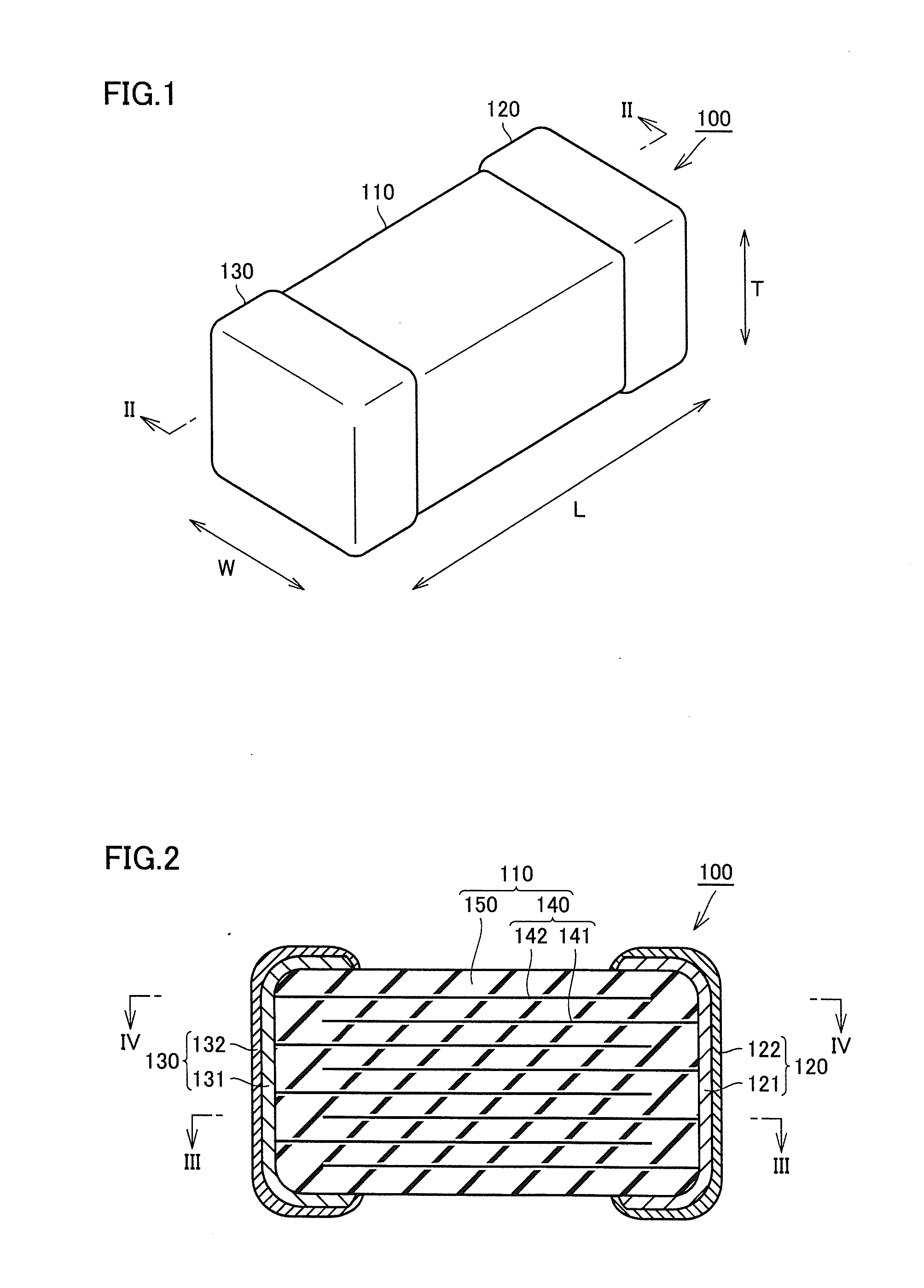
[0035]A ceramic electronic component according to preferred embodiments of the present invention will be described hereinafter with reference to the drawings. In the description of the preferred embodiments below, the same or corresponding elements in the drawings have the same reference numerals allotted and description thereof will not be repeated. Though a ceramic capacitor will be described as a ceramic electronic component in the description below, the electronic component is not limited to a capacitor, and the electronic component includes a piezoelectric component, a thermistor, or an inductor.

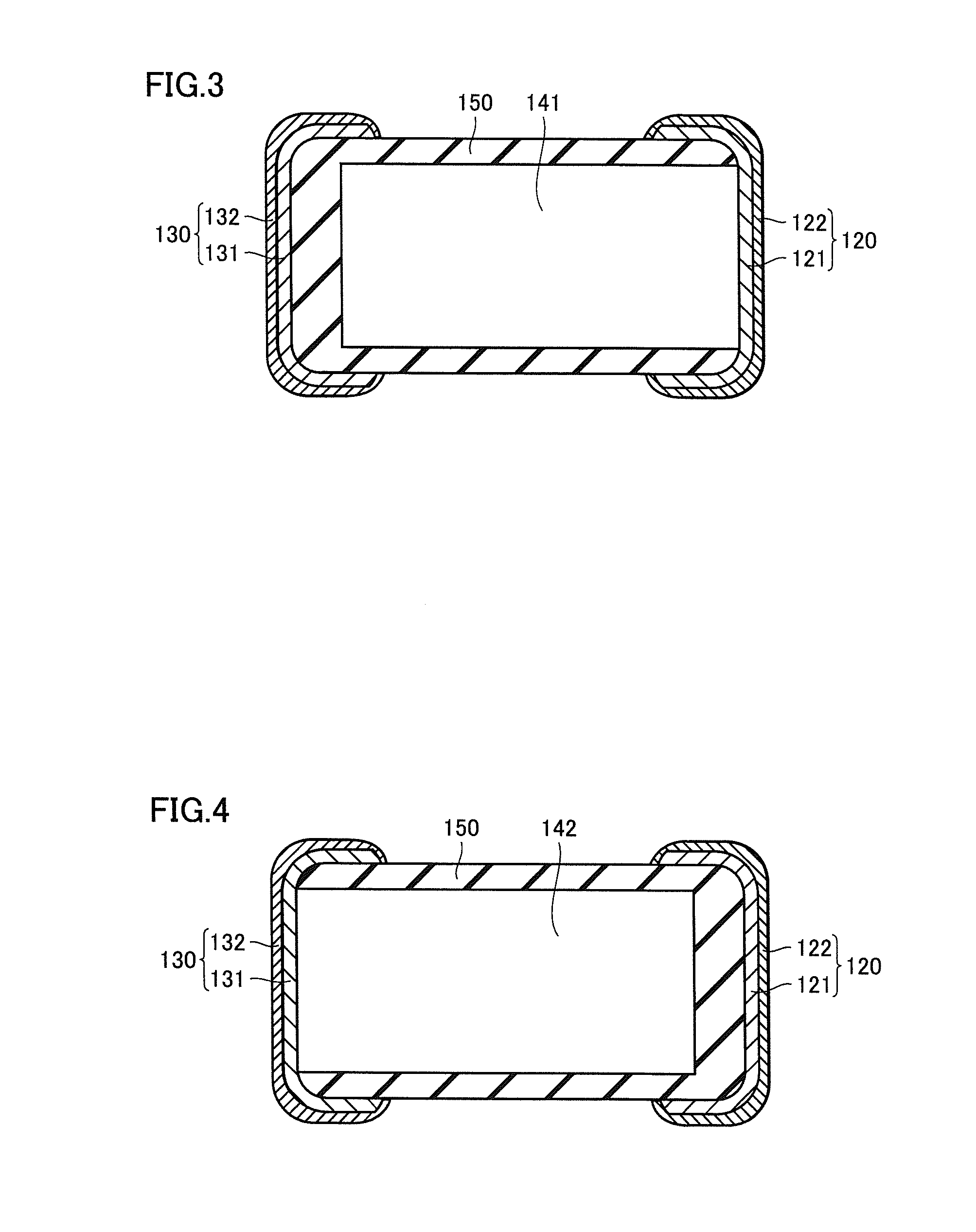
[0036]FIG. 1 is a perspective view showing an appearance of a ceramic electronic component according to a preferred embodiment of the present invention. FIG. 2 is a cross-sectional view of the ceramic electronic component in FIG. 1 viewed in a direction shown with an arrow along the line II-II. FIG. 3 is a cross-sectional view of the ceramic electronic component in FIG. 2 viewed in a di...


PUM

PropertyMeasurementUnit
depthaaaaaaaaaa
temperatureaaaaaaaaaa
melting pointaaaaaaaaaa

Abstract

A ceramic electronic component includes a rectangular or substantially rectangular parallelepiped shaped laminate in which a ceramic layer and an internal electrode are alternately laminated and an external electrode provided on a portion of a surface of the laminate and electrically connected to the internal electrode. The external electrode includes an inner external electrode covering a portion of the surface of the laminate and including a mixture of a resin component and a metal component and an outer external electrode covering the inner external electrode and including a metal component. The inner external electrode includes, as a metal component, a first metal component of which a portion forms an alloy with the internal electrode so as to connect the internal electrode and the inner external electrode to each other, and a second metal component higher in melting point than the first metal component, of which a portion forms an alloy with the first metal component so as to connect the inner external electrode and the outer external electrode to each other. A concentration of a metal in a surface layer of the inner external electrode is not lower than about 17%.

Description

BACKGROUND OF THE INVENTION[0001]1. Field of the Invention[0002]The present invention relates to a ceramic electronic component and a method of manufacturing the same.[0003]2. Description of the Related Art[0004]Ceramic electronic components including laminated ceramic capacitors have recently been used in an environment that is more severe than in a conventional example.[0005]For example, electronic components included in mobile devices such as a portable telephone and a portable music player are required to be resistant to shock at a time of being dropped. Specifically, electronic components are required not to be detached from a mounting board and to be free from cracks when a drop impact is applied thereto.[0006]Electronic components included in car-mounted devices such as an ECU (Engine Control Unit) are required to be resistant to shock originating from a heat cycle. Specifically, electronic components are required to be free from cracks in solder used for mounting and in the ...

Claims


Application Information

Patent Timeline
Patent Type & Authority Applications(United States)
IPC IPC(8): H01C7/00H01G4/008H01G4/30H01L41/297H01L41/047H01F41/04H01C17/00H01G4/12H01F27/28
CPCH01C7/008H01G4/12H01G4/008H01G4/30H01F2027/2809H01L41/0471H01F41/041H01C17/00H01L41/297H01F27/2804H01F17/0013H01F27/292H01F41/046H01C1/148H01C7/18H01G4/232H01G4/2325Y10T29/42Y10T29/4902Y10T29/43Y10T29/49085H10N30/872H10N30/877H10N30/063
Inventor HAMANAKA, KENICHIZENZAI, KOTADEKURA, TAKUMAEKAWA, KIYOTAKA
Owner MURATA MFG CO LTD
Why Eureka
Try Eureka