Method for measuring overlay and measuring apparatus, scanning electron microscope, and GUI

a scanning electron microscope and overlay technology, applied in the direction of instruments, semiconductor/solid-state device details, image enhancement, etc., can solve the problems of reducing yield, unable to directly measure overlay, and unable to obtain proper electric characteristics, etc., to achieve easy and robust measurement

Active Publication Date: 2014-12-25
HITACHI HIGH-TECH CORP
View PDF5 Cites 31 Cited by
  • Summary
  • Abstract
  • Description
  • Claims
  • Application Information

AI Technical Summary

Benefits of technology

[0013]According to the present invention, it is possible to provide a method for measuring overlay and a measuring apparatus, in which the overlay of the actual patterns can be measured easily and robustly without necessity of using the CAD data except for captured images and without inputting any reference value of the relative position.
[0014]The problems to be solved, configurations, and advantageous effects other than those described above will be clarified by embodiments described below.

Problems solved by technology

In the case where the positions of the circuit patterns cannot be adjusted within the permissible range, proper electric characteristic cannot be obtained and yield is decreased.
Therefore, the overlay cannot be directly measured in a place where the circuit patterns of an actual device (actual patterns) are formed, and it is necessary to estimate the overlay by interpolation or the like.
However, due to recent micro-miniaturization in the semiconductor process, the permissible range of the overlay is becoming more reduced and it is difficult to obtain necessary measurement accuracy.

Method used


Image

  • Method for measuring overlay and measuring apparatus, scanning electron microscope, and GUI
  • Method for measuring overlay and measuring apparatus, scanning electron microscope, and GUI
  • Method for measuring overlay and measuring apparatus, scanning electron microscope, and GUI

Examples


first embodiment

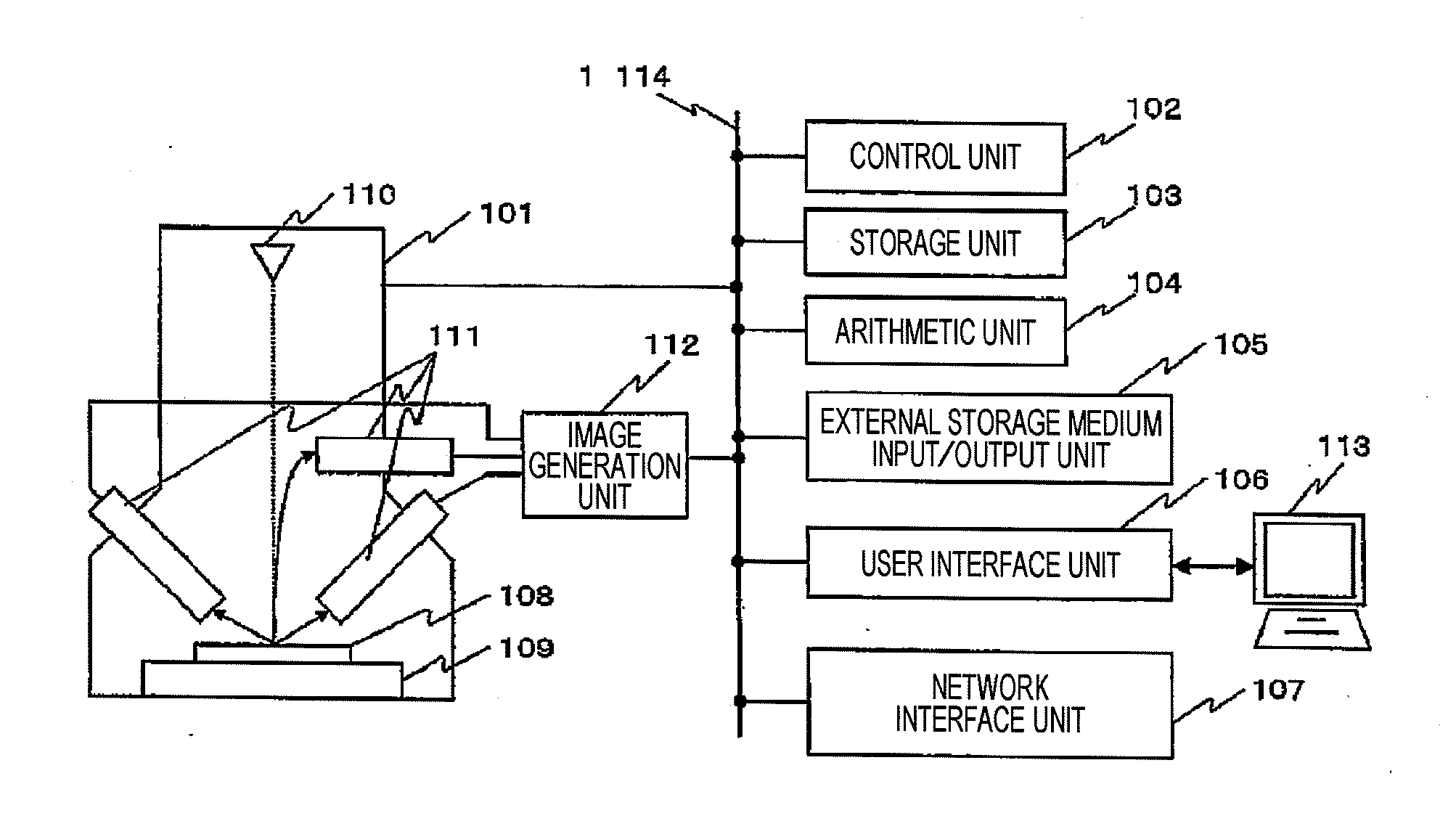
[0047]An overlay measuring apparatus and a measuring method according to the present invention will be described below. According to the present embodiment, a description will be given for a case in which overlay is measured by using an image captured by a scanning electron microscope (SEM) including an overlay measurement unit. However, an imaging device according to the present invention may be other than the SEM, for example, an imaging device using charged particle radiation such as ions.

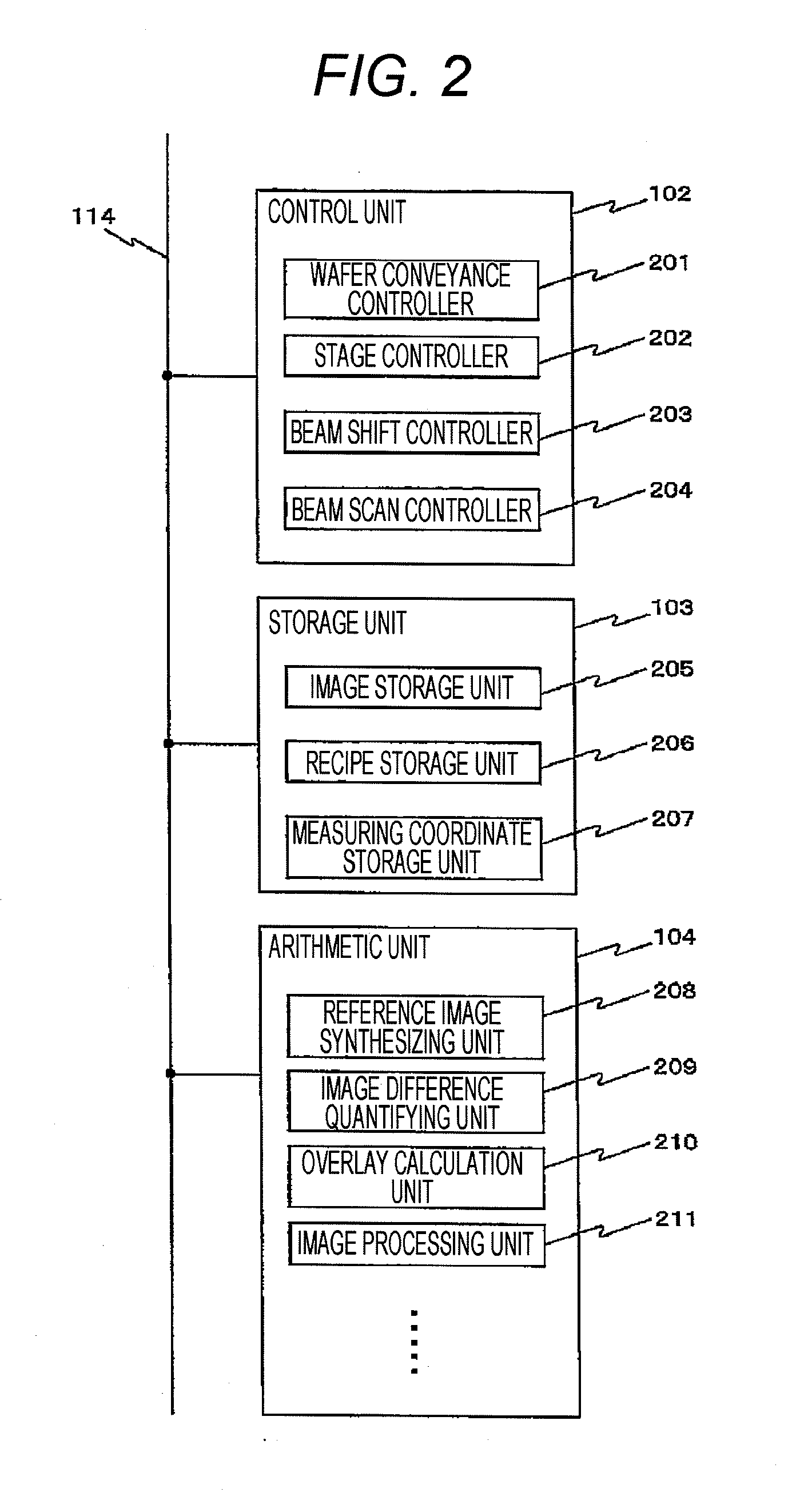
[0048]FIG. 1 is a diagram illustrating a configuration of the scanning electron microscope (SEM) including the overlay measuring apparatus according to the present invention, and the SEM includes an SEM 101 that captures an image of an object to be checked, a control unit 102 that executes total control, a storage unit 103 that stores image capturing results, etc. in a magnetic disk, a semiconductor memory or the like, an arithmetic unit 104 that performs computing in accordance with a program, ...

second embodiment

[0101]According to the first embodiment, a method in which overlay is measure by recognizing a circuit pattern area for each of a reference image and a measurement target image and quantifying a positional deviation amount for each circuit pattern formed by each exposure has been described. According to a second embodiment, a method in which the overlay is measured by recognizing the circuit pattern area only for the reference image and quantifying the positional deviation amount per each circuit pattern formed by each exposure will be described.

[0102]A configuration of an apparatus according to the present embodiment is same as those illustrated in FIGS. 1 and 2. Also, measurement flows are same as those illustrated in FIGS. 6 and 7. Further, interfaces are also same as those illustrated in FIGS. 15, 16 and 17. Matters different are a configuration of an image difference quantifying unit 209 (corresponding to 801 in FIG. 8) and a flow of image difference quantifying processing. In ...

third embodiment

[0108]According to the first and second embodiments, overlay measuring methods in which the overlay is measured recognizing a circuit pattern area from a reference image as well as a measurement target image and a positional deviation amount is quantified for each circuit pattern formed by each exposure has been described. According to a third embodiment, a method in which the overlay is measured by quantifying a difference of a gray value in an image between the reference image and the measurement target image will be described.

[0109]According to this method, a pixel size is enlarged by widening a visual field of the image. Accordingly, the method is effective in the case where it is hard to automatically recognize the circuit pattern area.

[0110]A configuration of an apparatus according to the present embodiment is same as FIG. 1. Also, a measurement flow is same as those illustrated in FIGS. 6 and 7. Further, interfaces are also same as those illustrated in FIGS. 15 and 16. Compar...


PUM


Abstract

A method for measuring overlay at a semiconductor device on which circuit patterns are formed by a plurality of exposure processes is characterized in including an image capturing step for capturing images of a plurality of areas of the semiconductor device, a reference image setting step for setting a reference image based on a plurality of the images captured in the image capturing step, a difference quantifying step for quantifying a difference between the reference image set in the reference image setting step and the plurality of images captured in the image capturing step, and an overlay calculating step for calculating the overlay based on the difference quantified in the difference quantifying step.

Description

TECHNICAL FIELD[0001]The present invention relates to a method for measuring overlay and a measuring apparatus, a scanning electron microscope, and a GUI, more specifically, relating to the method and apparatus for measuring the overlay by using an image captured by a charged particle microscope.BACKGROUND ART[0002]Generally, multiple times of exposure processes are necessary for semiconductor products in order to form circuit patterns required for operation. For example, in the case of manufacturing a semiconductor product formed of a plurality of layers of the circuit patterns, the exposure processes are necessary to be performed to form holes for connecting the respective layers in addition to the exposure processes to form the respective layers of the circuit patterns. Further, in recent years, double patterning is performed in order to form fine circuit patterns with high density.[0003]In the semiconductor manufacturing, it is important to adjust, within a permissible range, po...

Claims


Application Information

Patent Timeline
Patent Type & Authority Applications(United States)
IPC IPC(8): G06T7/00
CPCG06T7/001G06T2200/24G06T2207/30148G06T2207/10061G03F7/70633H01L23/544H01L2223/54453H01L22/12H01L2924/0002H01L2924/00
Inventor HARADA, MINORUNAKAGAKI, RYOFUKUNAGA, FUMIHIKOTAKAGI, YUJI
Owner HITACHI HIGH-TECH CORP
Why Eureka
Try Eureka