

Surface measurement device
a measurement device and surface technology, applied in the direction of semiconductor/solid-state device testing/measurement, instruments, semiconductor materials, etc., can solve the problem of substantially impossible in-line measurement of an entire surface of a wafer
- Summary
- Abstract
- Description
- Claims
- Application Information
AI Technical Summary
Benefits of technology
Problems solved by technology
Method used
Image

Examples
first embodiment
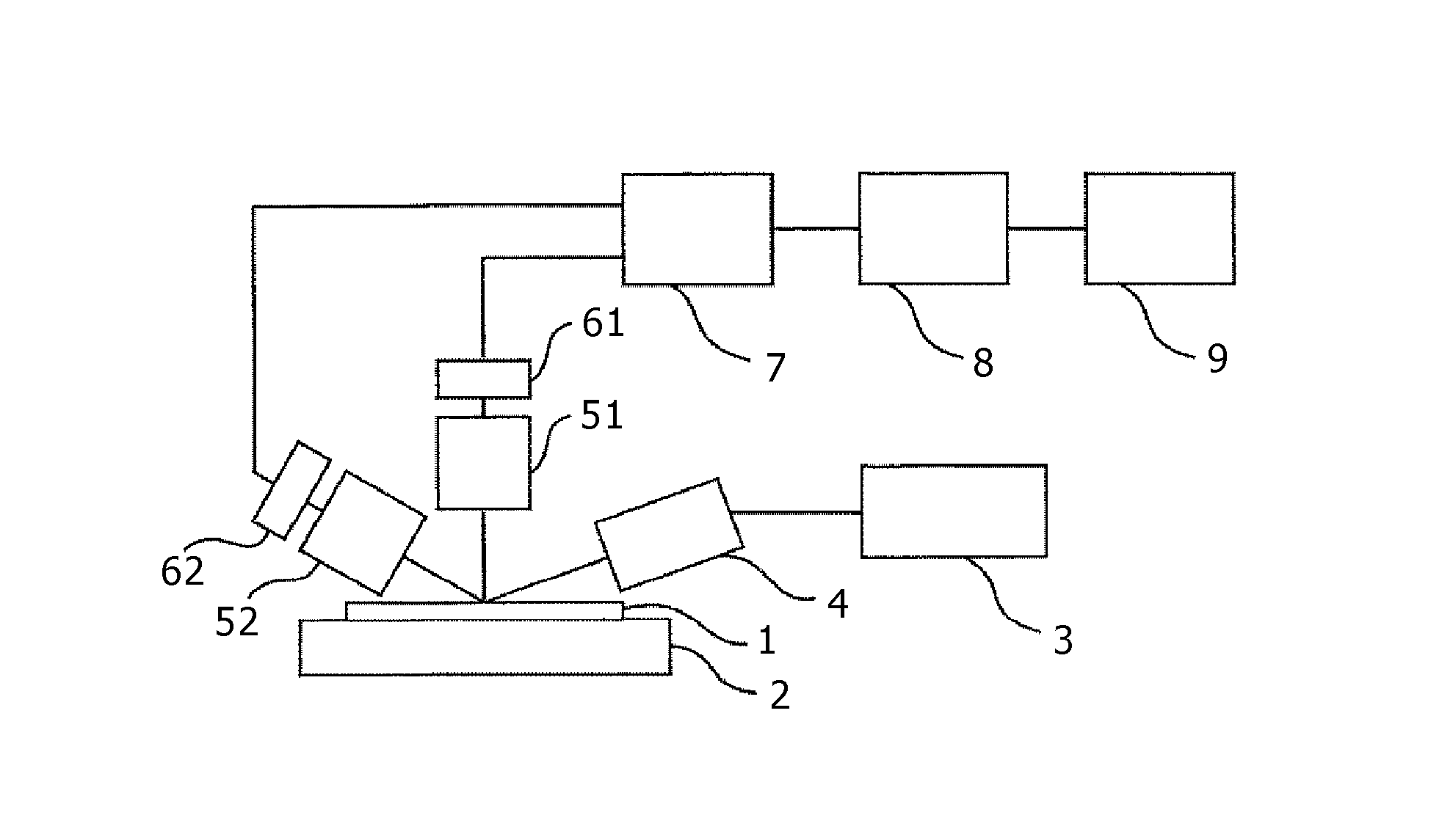
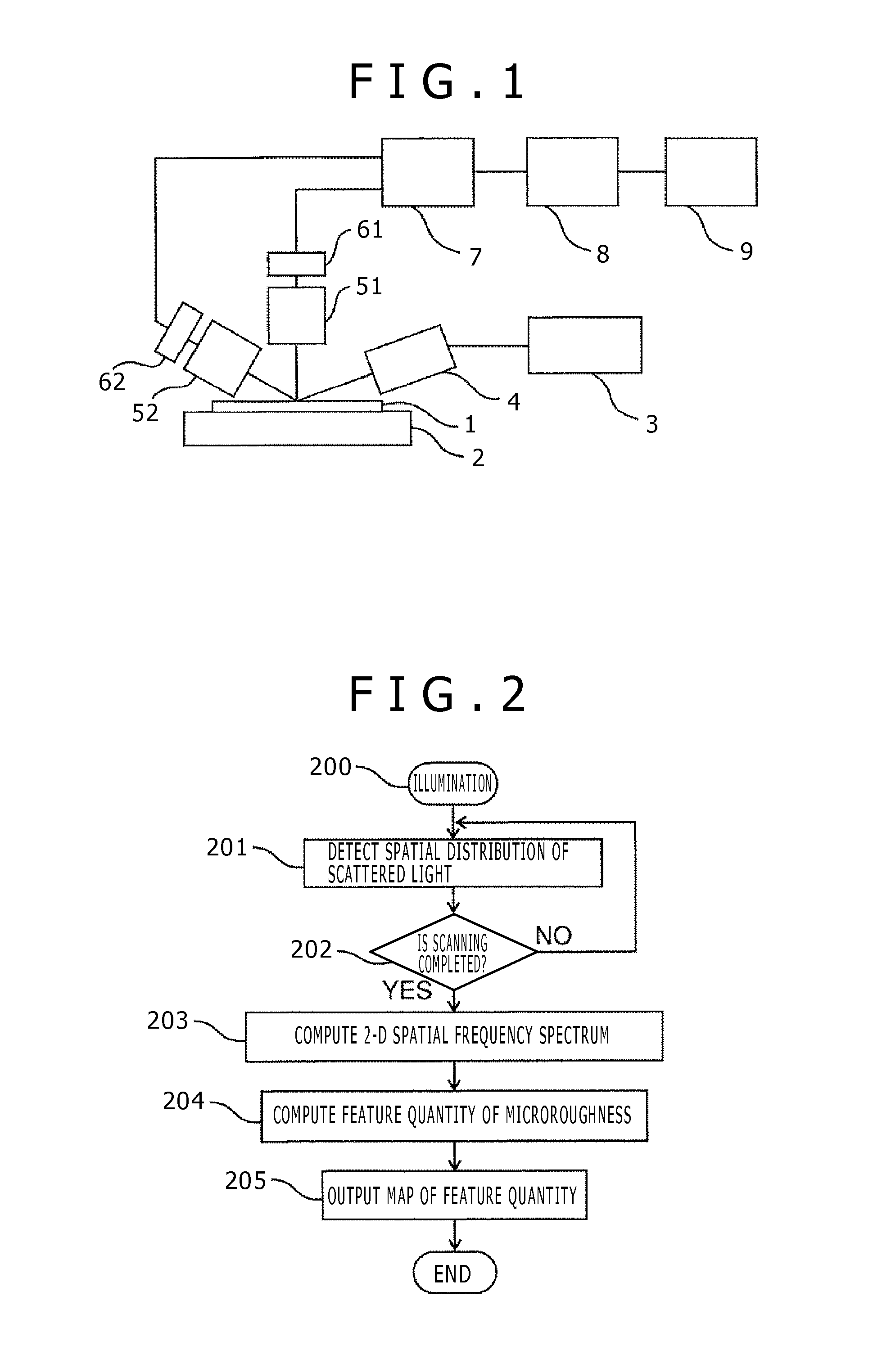
[0063]As one embodiment of the present invention, a measurement device of microroughness of a wafer surface in semiconductor device manufacture will be explained. FIG. 1 shows an outline configuration of the surface measurement device. Its main components are a stage 2 that mounts thereon a wafer 1, alight source 3, an illumination optical system 4 having lenses, mirrors, etc., detection optical systems 51 to 59 (53 to 59 are not illustrated) that have lenses, mirrors, etc., photodetectors 61 to 69 (63 to 69 are not illustrated) for detecting light that is collected by the detection optical systems 51 to 59, a signal processing system 7, a control system 8, and an operation system 9. Incidentally, the detection optical systems 51 to 59 are arranged so that at least one of an elevation angle and an azimuth angle to the wafer 1 may be different. In connection with it, the photodetectors 61 to 69 are also arranged so that at least one of the elevation angle and the azimuth angle to the...
second embodiment
[0110]Next, a second embodiment will be explained. The second embodiment is one that expands a detectable spatial frequency range in contrast to the first embodiment.
[0111]FIG. 15 shows an arrangement of detection optical systems (apertures on the celestial sphere are projected onto a plane parallel to the wafer surface). The second embodiment has 13 detection optical systems and 13 photodetectors corresponding to them. That is, detection apertures 110 to 113 are supplemented to the first embodiment. The detection apertures 110 and 111 are configured to be symmetrical relative to the plane of incidence, and the detection apertures 112 and 113 are configured to be symmetrical relative to the plane of incidence.
[0112]By the arrangement of the detection optical systems like this, a detectable spatial frequency range can be expanded. As a result, it becomes possible to grasp a variation of the 2-D spatial frequency spectrum sensitively, which improves the measurement accuracy of the mic...
third embodiment
[0113]Next, a third embodiment will be explained. The third embodiment improves the resolution of detectable spatial frequency in contrast to the first embodiment and the second embodiment.
[0114]FIG. 16 shows the scattered light detection by a set of a detection optical system and a photodetector. A point that illumination light 1601 is irradiated to the wafer 1 is the same as the first embodiment and the second embodiment. In the third embodiment, the detection optical system that was referred to in the first embodiment and the second embodiment is substituted with a Fourier transform optical system 1602. The Fourier transform optical system 1602 collects scattered light 1603 diverging from the wafer, and emits parallel light 1604. Then, the parallel light is detected by a 2-D sensor 1605. As the 2-D sensor, a charge-coupled device (CCD), a time delay integral sensor (TDI), a multi-pixel photon counter, an avalanche photodiode array, etc. can be used. After the scattered light is d...
PUM
 Abstract
Description
Claims
Application Information