LED Package and Method of the Same

a technology of led packaging and lead frame, applied in the direction of solid-state devices, electric elements, electric apparatus, etc., can solve the problems of inability to meet the demand of producing smaller chips with high-density elements on the chip, the heat sink of the prior art is too large to scale down the package, etc., to achieve short conductive trace, low cost, and high performance

Inactive Publication Date: 2015-01-01
KING DRAGON INT
View PDF71 Cites 0 Cited by
  • Summary
  • Abstract
  • Description
  • Claims
  • Application Information

AI Technical Summary

Benefits of technology

[0006]An object of the present invention is to provide a LED package with a shorter conductive trace by low cost, high performance and high reliability package.
[0007]Another object of the present invention is to provide a convenient, cost-effective method for manufacturing a LED package (chip assembly) by using the bare LED chips as FIG. 8 without bump structure on the P & N electrode pads.
[0008]Another object of the present invention is to provide a good thermal management structure to offer the lowest thermal resistance from heat source (inside the chip−P / N junction) to the outside heat sink by using the cooper plug to contact the P / N junction directly without any adhesive materials due to the thermal conductivity of copper around 400 W / mK and using sputtering plus electro-plating method instead of the solder join method (the thermal conductivity of solder (Sn) around 20-80 W / mK).

Problems solved by technology

As a semiconductor become more complicated, the traditional package technique, for example lead frame package, flex package, rigid package technique, can't meet the demand of producing smaller chip with high density elements on the chip.
Due to the manufacturing technology and material requirements, packages having built-up layers often include a number of degassing holes in the metal layers.
Further, the heat sink of the prior art is too huge to scale down the package.

Method used


Image

  • LED Package and Method of the Same
  • LED Package and Method of the Same
  • LED Package and Method of the Same

Examples


Embodiment Construction

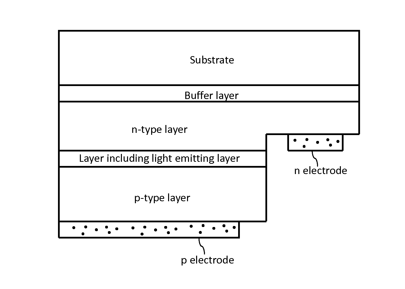
[0021]The invention will now be described in greater detail with preferred embodiments of the invention and illustrations attached. Nevertheless, it should be recognized that the preferred embodiments of the invention is only for illustrating. Besides the preferred embodiment mentioned here, present invention can be practiced in a wide range of other embodiments besides those explicitly described, and the scope of the present invention is expressly not limited expect as specified in the accompanying Claims. The present invention discloses a LED package assembly which includes LED die (element), conductive trace and metal inter-connecting as shown in FIG. 2.

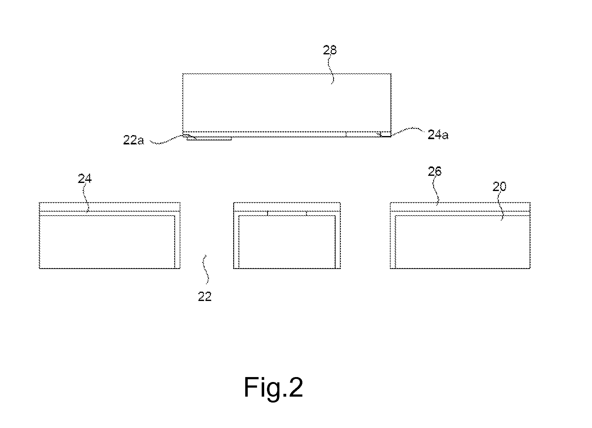
[0022]FIG. 2 is cross-sectional view of a substrate 20 with predetermined through-holes 22 formed therein. The substrate 20 could be a metal, glass, ceramic, silicon, plastic, BT, PCB or PI. The thickness of the substrate 20 is around 40-200 micron-meters. It could be a single or multi-layer (wiring circuit) substrate. A conductiv...


PUM


Abstract

LED package includes a substrate with pre-formed P-type through-hole and N-type through-hole through said substrate, wherein a conductive material formed on the sidewall of said P-type through-hole and N-type through-hole; a reflective layer formed on an upper surface of said substrate; a LED die having P-type pad and N-type pad aligned with said P-type through-hole and said N-type through-hole; said P-type pad and N-type pad being formed on a first surface of said LED die; wherein said LED die is formed on said upper surface of said substrate; a copper refilling material within said P-type through-hole and said N-type through-hole thereby forming electrical connection from said P-type pad and said N-type pad; and a P-type terminal pad under said substrate and electrical coupled to said P-type pad through said copper refilling material within said P-type through-hole, a N-type terminal pad under said substrate and electrical coupled to said N-type pad through said copper refilling material within said N-type through hole.

Description

FIELD OF THE INVENTION[0001]This invention relates to a LED package, and more particularly to LED package with through-hole structure and improved thermal dissipation.DESCRIPTION OF THE PRIOR ART[0002]High performance integrated circuit (IC) packages are well known in the art. Improvements in IC packages are driven by industry demands for increased thermal and electrical performance and decreased size and cost of manufacture. In the field of LED devices, it is required to be package as the IC device. The die density is increased and the device dimension is reduced, continuously. The demand for the packaging techniques in such high density devices is also increased to fit the situation mentioned above. Conventionally, in the flip-chip attachment method, an array of solder bumps is formed on the surface of the die. The formation of the solder bumps may be carried out by using a solder composite material through a solder mask for producing a desired pattern of solder bumps. The functio...

Claims


Application Information

Patent Timeline
Patent Type & Authority Applications(United States)
IPC IPC(8): H01L33/62H01L33/60
CPCH01L33/60H01L2933/0058H01L33/62H01L24/19H01L33/486H01L33/641H01L33/647H01L2224/48091H01L2224/48247H01L2924/3011H01L2933/0066H01L2224/8592H01L2924/00014H01L2924/12042H01L2924/181H01L24/20H01L24/48H01L2224/92144H01L2924/00H01L2224/45099H01L2924/00012
Inventor YANG, WEN KUNYANG, YU-HSIANG
Owner KING DRAGON INT
Why Eureka
Try Eureka