Multi-layer 3D pattern manufacturing method and manufacturing apparatus thereof
- Summary
- Abstract
- Description
- Claims
- Application Information
AI Technical Summary
Benefits of technology
Problems solved by technology
Method used
Image
Examples
first preferred embodiment
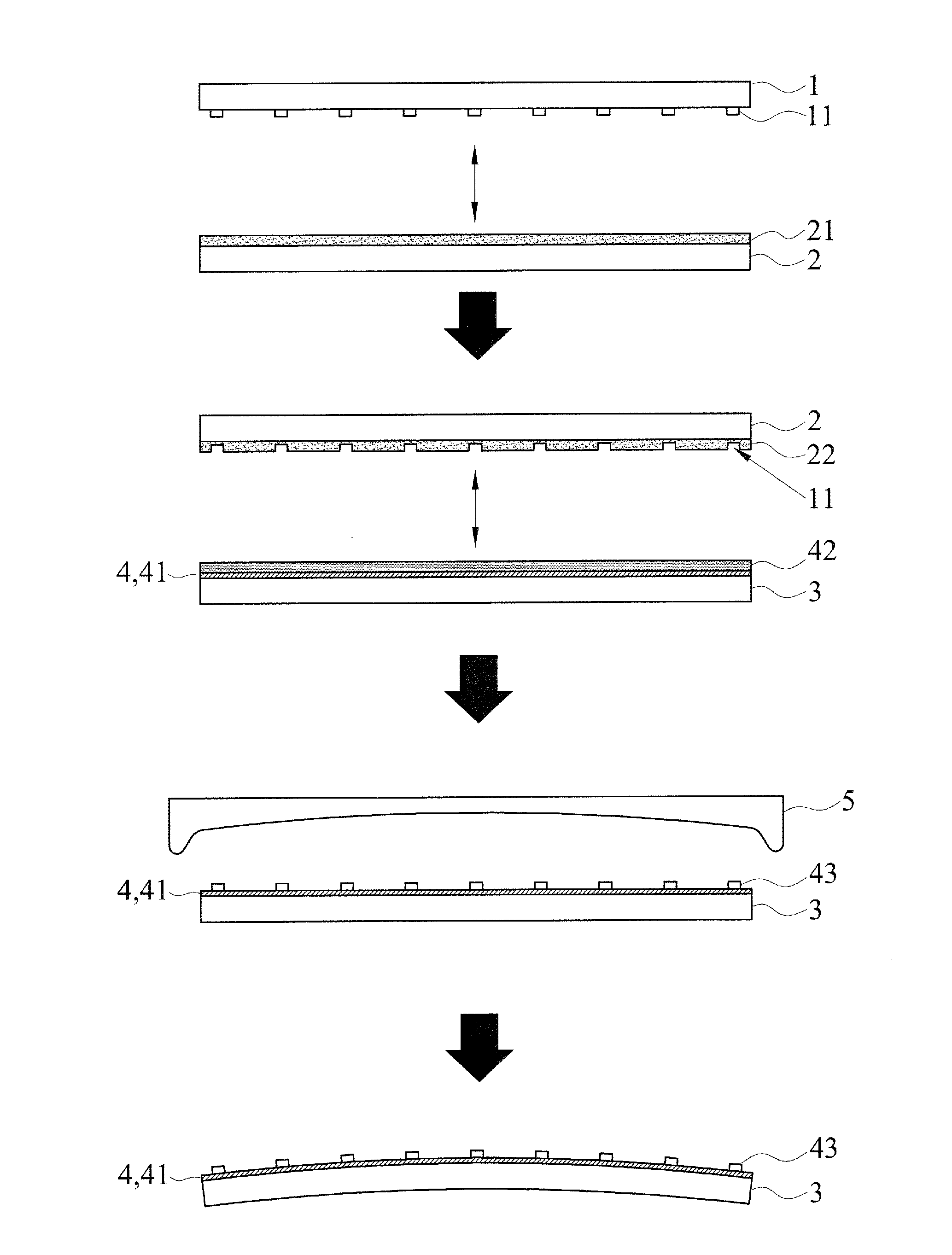
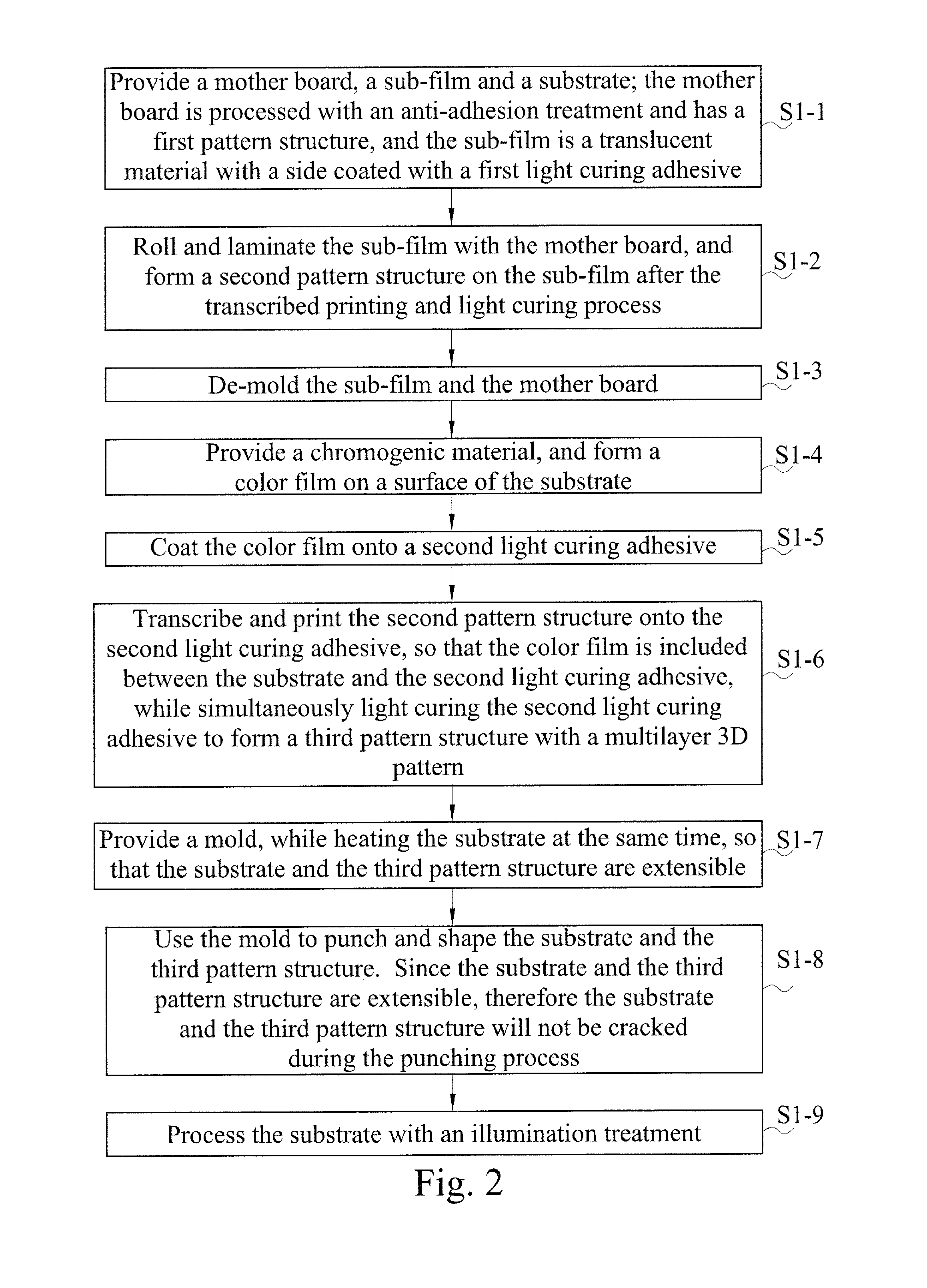
[0034]With reference to FIGS. 2 and 3 for a flow chart and a schematic view of the first preferred embodiment of the present invention respectively, a multi-layer 3D pattern manufacturing method of the first preferred embodiment of the present invention comprises the following steps:
[0035]S1-1: Provide a mother board 1, a sub-film 2 and a substrate 3, wherein the mother board 1 is processed with an anti-adhesion treatment and has a first pattern structure 11, and the sub-film 2 is a translucent material with a side coated with a first light curing adhesive 21. It is noteworthy that the mother board 1 is a flat board made of material selected from anyone of stainless steel, electroformed plate and quartz glass. And the first pattern structure 11 of the mother board 1 is manufactured by methods such as etch molding, laser engraving, drill molding, or sand-blast molding to create patterns with different depths, widths, intervals, surface glosses (roughness) and angles to meet the patte...
second preferred embodiment
[0045]With reference to FIGS. 4A, 4B and 5 for a flow chart and a schematic view of the second preferred embodiment of the present invention respectively, the materials used in the multi-layer 3D pattern manufacturing method of the second preferred embodiment of the present invention are the same as those of the first preferred embodiment, but the steps are slightly different, so that the same numerals are the same elements in both embodiments. The multi-layer 3D pattern manufacturing method of the second preferred embodiment of the present invention comprises the following steps:
[0046]S2-1: Provide a mother board 1, a sub-film 2 and a substrate 3, wherein the mother board 1 is processed with an anti-adhesion treatment and has a first pattern structure 11, and the sub-film 2 is a translucent material with a side coated with a first light curing adhesive 21, and a side of the substrate 3 is coated with a second light curing adhesive 42.
[0047]S2-2: Roll and laminate the sub-film 2 wit...
PUM
| Property | Measurement | Unit |
|---|---|---|
| Temperature | aaaaa | aaaaa |
| Color | aaaaa | aaaaa |
| Height | aaaaa | aaaaa |
Abstract
Description
Claims
Application Information


