Solar cell module and method of fabricating the same

a solar cell and module technology, applied in the field of solar cell modules, can solve the problems of difficult control of mocvd deposition uniformity and toxic cadmium (cd) toxicity, and achieve the effects of reducing damage and pin holes, improving photoelectric conversion efficiency, and increasing open-circuit voltage vo

Inactive Publication Date: 2015-01-29
LG INNOTEK CO LTD
View PDF2 Cites 1 Cited by
  • Summary
  • Abstract
  • Description
  • Claims
  • Application Information

AI Technical Summary

Benefits of technology

[0012]According to the solar cell module of the embodiment, the second buffer layer is formed between the first buffer layer and the front electrode layer. The second buffer layer can reduce the damage and pin holes, which may be generated in the first buffer layer in the process of forming the front electrode layer, and can prevent the shunt to increase the open-circuit voltage Voc.
[0013]In addition, the bandgap energy Eg of the second buffer layer has the intermediate value between the bandgap energy of the first buffer layer and the bandgap energy of the front electrode layer. That is, according to the embodiment, the bandgap of the second buffer layer can be aligned with the bandgaps of adjacent layers, so the recombination of the electron-hole can be minimized and the photoelectric conversion efficiency can be improved.

Problems solved by technology

However, there are disadvantages that cadmium (Cd) has toxicity and the buffer layer is manufactured through a wet process, such as chemical bath deposition (CBD).
In general, it is difficult to control the deposition uniformity in the MOCVD process when comparing with the sputtering process.

Method used


Image

  • Solar cell module and method of fabricating the same
  • Solar cell module and method of fabricating the same
  • Solar cell module and method of fabricating the same

Examples


first embodiment

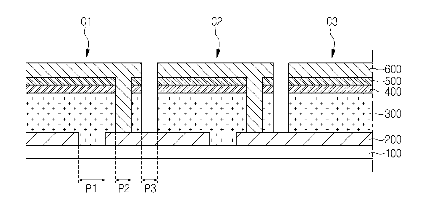
[0018]FIG. 1 is a sectional view showing a solar cell module according to the

[0019]Referring to FIG. 1, a solar cell according to the first embodiment includes a support substrate 100, a back electrode layer 200, a light absorbing layer 300, a first buffer layer 400, a second buffer layer 500, and a front electrode layer 600.

[0020]The support substrate 100 has a plate shape and supports the back electrode layer 200, the light absorbing layer 300, the first buffer layer 400, the second buffer layer 500, and the front electrode layer 600.

[0021]The support substrate 100 may be an insulator. For example, the support substrate 100 may be a glass substrate, a plastic substrate or a metal substrate. In detail, the support substrate 100 may be a soda lime glass substrate. The support substrate 100 may be transparent. The support substrate 100 may be rigid or flexible.

[0022]The back electrode layer 200 is a conductive layer. The back electrode layer 200 may include at least one of molybdenum...

second embodiment

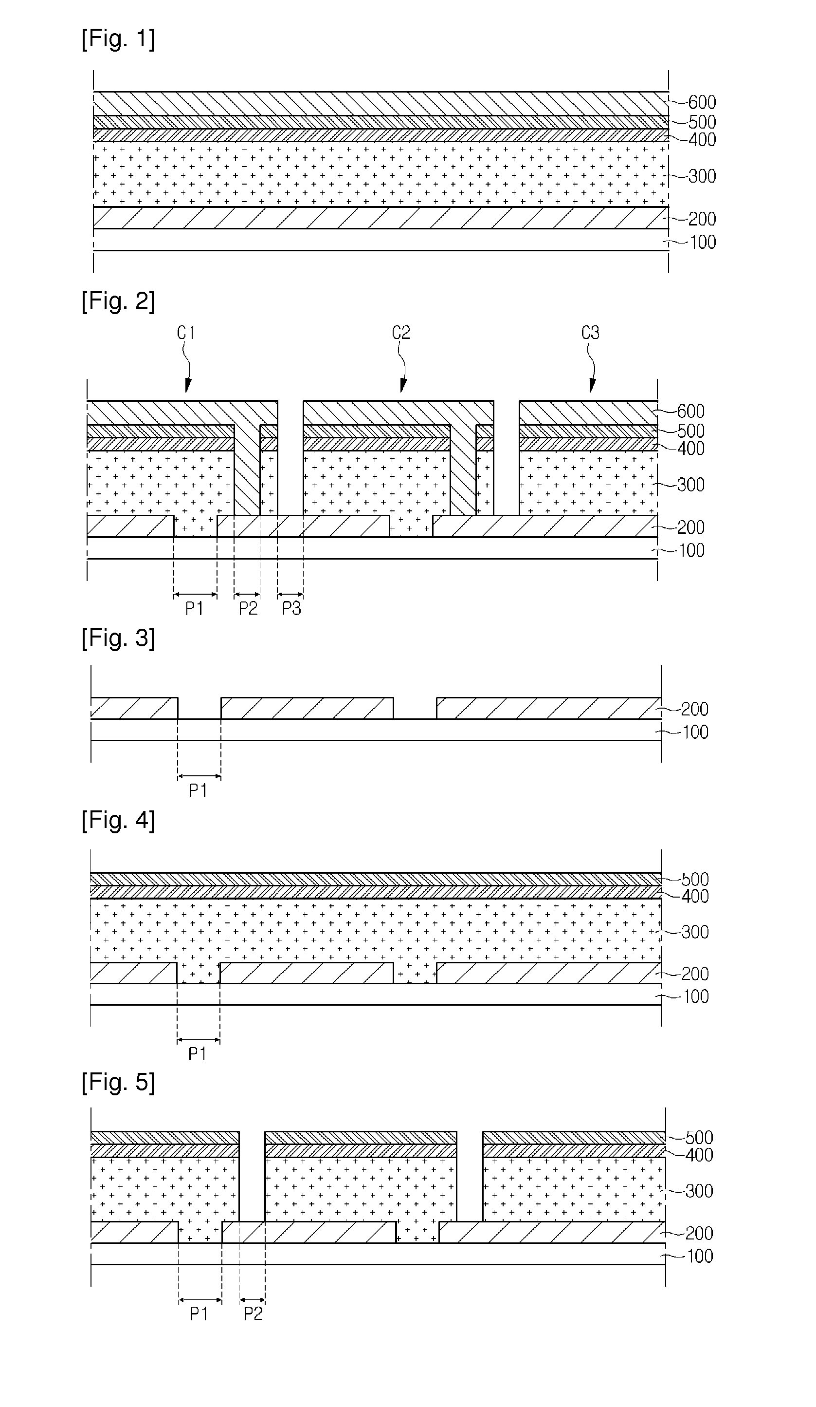
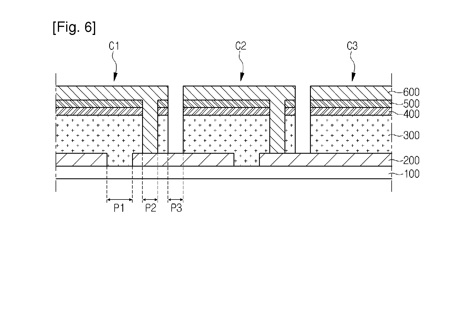
[0037]FIG. 2 is a sectional view showing a solar cell module and FIGS. 3 to 6 are sectional views showing a method of fabricating a solar cell module according to the embodiment.

[0038]Referring to FIG. 2, the solar cell module according to the second embodiment incudes a front electrode layer 200 disposed on a support substrate 100 and formed with a first through hole P1 for exposing a portion of the support substrate 100; a light absorbing layer 300 formed on the first through hole P1 and the back electrode layer 200; a first buffer layer 400 formed on the light absorbing layer 300 and expressed as chemical formula 1; a second through hole P2 formed through the light absorbing layer 300 and the first buffer layer 400 to expose a portion of the back electrode layer 200; a second buffer layer 500 formed on the first buffer layer 400 and expressed as chemical formula 2; and a front electrode layer 600 formed on the second buffer layer 500 and gap-filled in the second through hole P2....


PUM


Abstract

Disclosed are a solar cell module and a method of fabricating the same. The solar cell module includes a back electrode layer on a support substrate; a light absorbing layer on the back electrode layer; a first buffer layer on the light absorbing layer; a second buffer layer on the buffer layer; and a front electrode layer on the second buffer layer.

Description

TECHNICAL FIELD[0001]The embodiment relates to a solar cell module and a method of fabricating the same.BACKGROUND ART[0002]Solar cells may be defined as devices to convert light energy into electrical energy by using a photovoltaic effect of generating electrons when light is incident onto a P-N junction diode. The solar cell may be classified into a silicon solar cell, a compound semiconductor solar cell mainly including a group I-III-VI compound or a group III-V compound, a dye-sensitized solar cell, and an organic solar cell according to materials constituting the junction diode.[0003]A solar cell made from CIGS (CuInGaSe), which is one of group I-III-VI Chal-copyrite-based compound semiconductors, represents superior light absorption, higher photoelectric conversion efficiency with a thin thickness, and superior electro-optic stability, so the CIGS solar cell is spotlighted as a substitute for a conventional silicon solar cell.[0004]In general, a CIGS solar cell can be prepared...

Claims


Application Information

Patent Timeline
Patent Type & Authority Applications(United States)
IPC IPC(8): H01L31/0216H01L31/0224
CPCH01L31/022466H01L31/02167H01L31/0322H01L31/03923H01L31/0749Y02E10/541H01L31/046H01L31/0445H01L31/18
Inventor JEE, SUK JAE
Owner LG INNOTEK CO LTD
Why Eureka
Try Eureka