Lightweight carrier structure, particularly for optical components, and method for its production

a carrier structure and optical component technology, applied in the direction of machine supports, domestic objects, lamination, etc., can solve problems such as processing difficulties, and achieve the effect of small surface roughness and minimal surface roughness

Active Publication Date: 2015-01-29
ASML NETHERLANDS BV
View PDF2 Cites 0 Cited by
  • Summary
  • Abstract
  • Description
  • Claims
  • Application Information

AI Technical Summary

Benefits of technology

[0011]The inventors have found that the following advantages are achieved with the application of the anodic bonding for producing a carrier structure. First, the bond connection constitutes a firm bond between the carrier body and the cover layer, which firm bond is free from foreign material, such as e.g. glass solder or adhesive. The bond connection provides a high strength, with which the rigidity of the carrier structure is improved. The bond connection consists completely of inorganic materials, particularly materials which are extremely stable chemically. Advantageously, a degrading of the connection by means of outgassing, as can occur in the case of conventional adhesively bonded carrier structures, is excluded. Furthermore, the bond connection is resistant to highly energetic radiation, particularly to cosmic radiation or γ radiation. Therefore the long-term stability of the carrier structure is increased, which is of particular advantage for optical components for application in space, such as e.g. for mirrors for satellite communication.
[0023]The carrier body has hollows which are preferably formed by recesses in the material of the carrier body and / or by means of a porous structure of the carrier body. Advantageously, there are various variants for forming the hollows in the carrier body. Preferably, shaping takes place in a precursor state of the ceramic, in which the ceramic is not yet completely processed, particularly not yet hardened (so-called green-machining of the ceramic). For example, the structure is milled in SiSiC ceramic before the SiSiC ceramic is fired, sintered and infiltrated with Si. The formation of the hollows, e.g. with milling tools, is advantageously particularly simple in this precursor state. Possible deformations of the carrier body after the finishing of the ceramic, particularly after the firing and sintering, can be compensated by means of post-processing and / or the shaping of the at least one cover layer. Alternatively, the formation of the hollows can take place by means of a mechanical processing on the finished bulk material of the ceramic of the carrier body. The mechanical processing can comprise a milling, an erosion (spark erosion), sandblasting and / or water / sandblasting.

Problems solved by technology

On the one hand, the carrier body has the desired strength and stability as well as a high potential for weight reduction by means of a high aspect ratio (volume of the hollows:volume of the carrier body material), wherein however, the hardness and microscopic roughness of the ceramic carrier body makes processing difficult, particularly for forming optically reflective surfaces.

Method used


Image

  • Lightweight carrier structure, particularly for optical components, and method for its production
  • Lightweight carrier structure, particularly for optical components, and method for its production
  • Lightweight carrier structure, particularly for optical components, and method for its production

Examples


Embodiment Construction

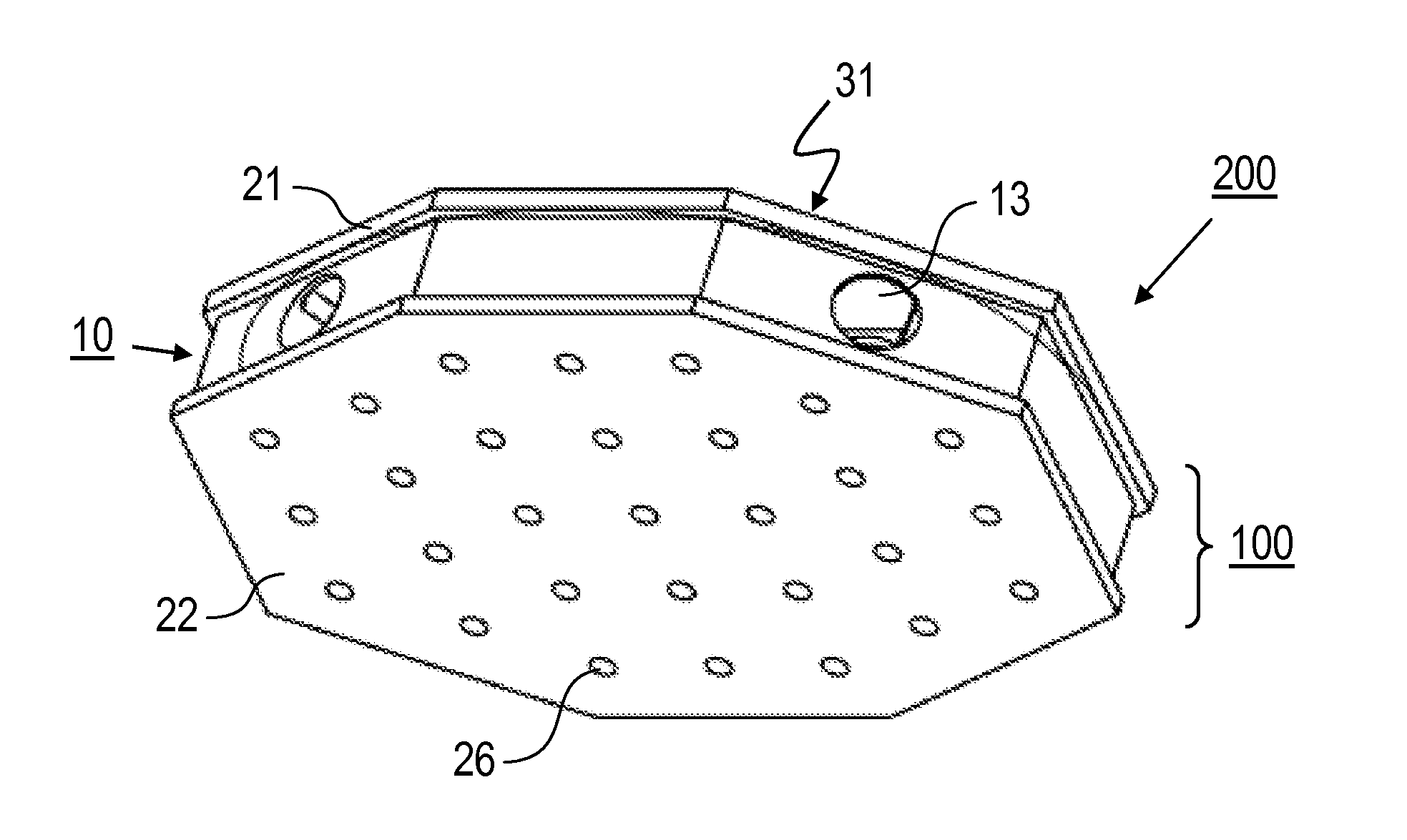
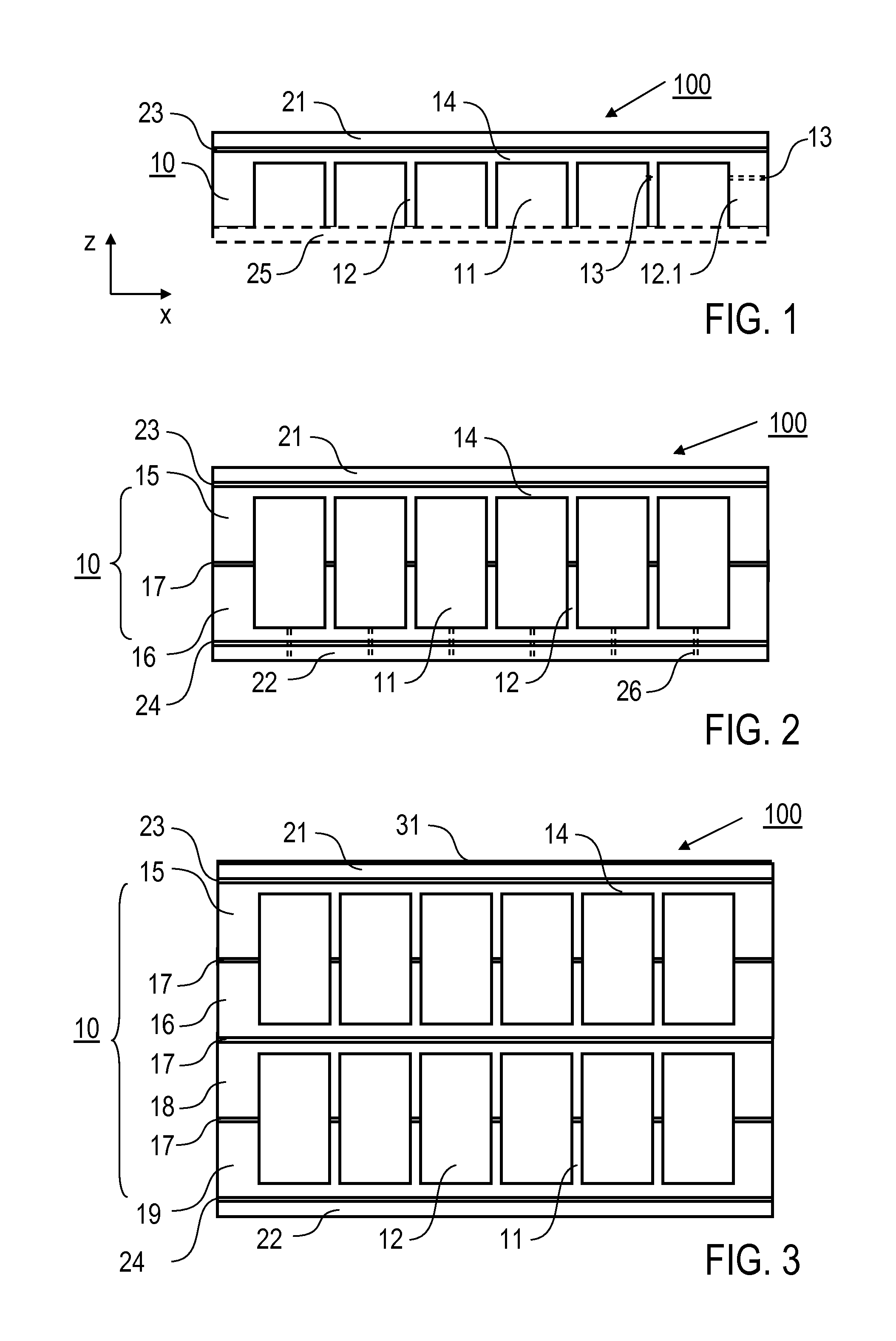
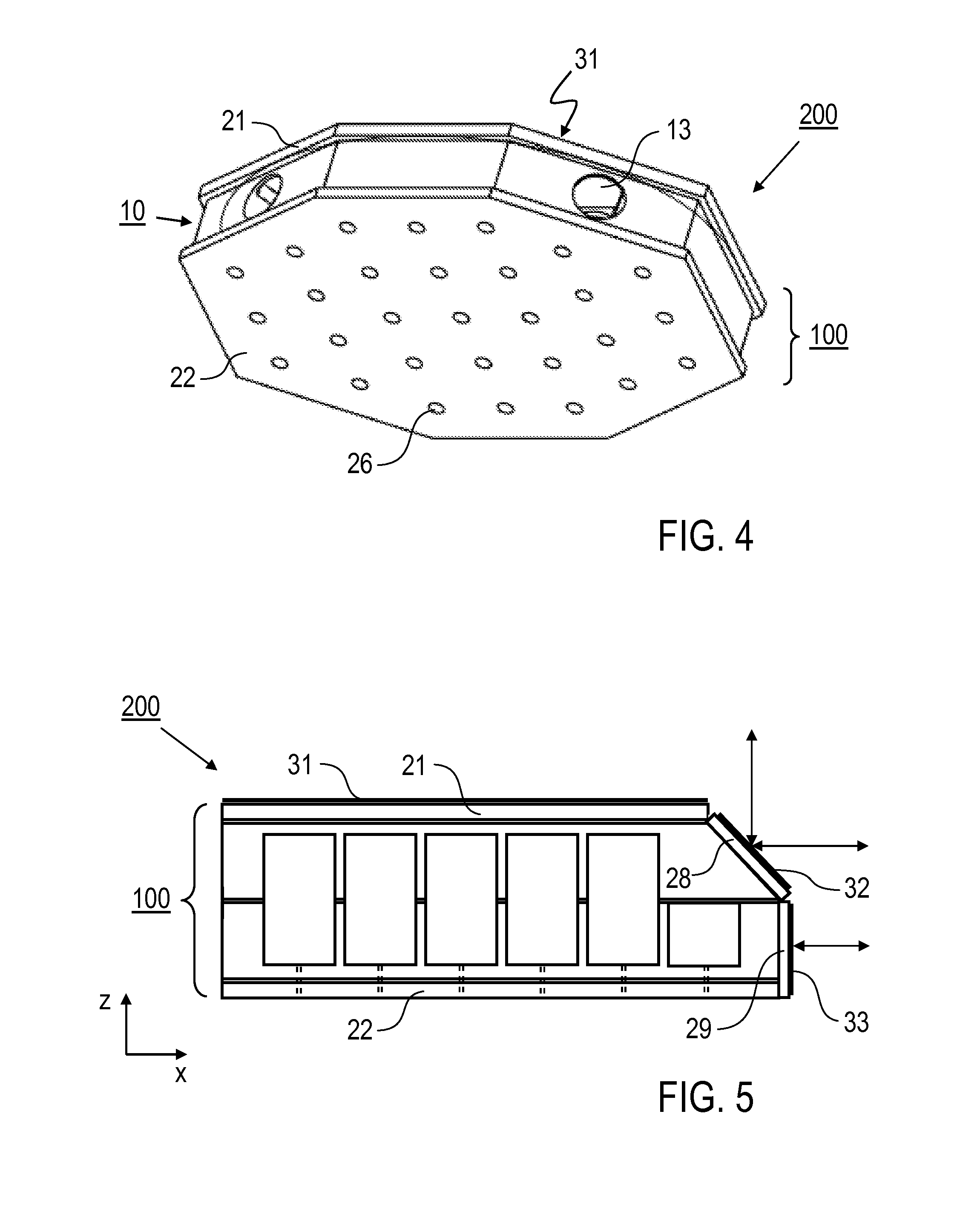
[0030]FIGS. 1 to 3 illustrate embodiments of the carrier structure 100 according to the invention in a schematic sectional view which is not to scale. The carrier structure 100 comprises a carrier body 10 and at least one cover layer 21, 22 which is connected to surfaces of the carrier body 10 on one or both sides by means of at least one bond connection 23, 24.

[0031]The carrier body 10 consists of an electrically conductive ceramic, e.g. SiSiC ceramic, in which hollows 11 are formed. For applications of the carrier structure as a mirror block, e.g. in a CPA system or a telescope, the thickness of the carrier body 10 is preferably selected in the range from 1 cm to 10 cm. The hollows 11 extend in the thickness direction (z direction) through the carrier body 10 in such a manner that a side wall 14 closed in the lateral direction (x direction) remains closed on one side of the carrier body 10. The side walls 14 form the main surfaces of the carrier body 10. All hollows 11 can have th...


PUM

PropertyMeasurementUnit
temperatureaaaaaaaaaa
thicknessaaaaaaaaaa
thicknessaaaaaaaaaa

Abstract

A carrier structure (100), particularly for optical components, includes a carrier body (10) which is formed from ceramic with hollows (11), and at least one cover layer (21, 22) which is formed from glass, arranged on at least one surface of the carrier body (10), and is connected to the carrier body (10) by means of at least one bond connection (23, 24) produced by means of anodic bonding. Methods for producing the carrier structure (100) and the use of the carrier structure as a mirror body, carrier for optical components and / or mechanical carrier for dynamically moved components are also described.

Description

BACKGROUND[0001]The invention relates to a carrier structure, particularly for optical components, comprising a carrier body with hollows (hollow spaces) and at least one cover layer which is arranged on at least one surface of the carrier body. The invention relates in particular to a lightweight carrier structure for an optical mirror or for a dynamically movable carrier platform, e.g. for optical components. The invention also relates to a method for producing a carrier structure of this type. Applications of the invention exist in particular in the case of the production of optical components or carriers for optical components.[0002]A lightweight carrier structure is a mechanical component, the mass of which is minimized by means of the formation of hollows in a carrier body of the carrier structure. A hollow honeycomb structure, which is characterized by a high mechanical stability, can be formed for example in the carrier body. Applications of lightweight carrier structures ex...

Claims


Application Information

Patent Timeline
Patent Type & Authority Applications(United States)
IPC IPC(8): G02B7/182C04B37/04F16M13/00
CPCF16M13/00G02B7/182F16M2200/08C04B37/042C04B37/045C04B2237/10C04B2237/12C04B2237/365G02B7/183
Inventor BALDUS, OLIVERSCHMIDT, VOLKER
Owner ASML NETHERLANDS BV
Why Eureka
Try Eureka