Bipolar transistor, semiconductor device, and bipolar transistor manufacturing method

a manufacturing method and semiconductor technology, applied in semiconductor devices, semiconductor/solid-state device details, electrical devices, etc., can solve problems such as etching anisotropy

Inactive Publication Date: 2015-02-05
MURATA MFG CO LTD
View PDF6 Cites 6 Cited by
  • Summary
  • Abstract
  • Description
  • Claims
  • Application Information

AI Technical Summary

Benefits of technology

[011], a cross-section perpendicular to the short-side direction has an inverted mesa shape, and a cross-section perpendicular to the long-side direction has a forward mesa shape; a base layer that is formed on the collector layer; a base electrode that is formed on the base layer; and a base line that is connected to the base electrode and that is drawn out from an end in the short-side direction of the collector layer to the outside of the collector layer in a plan view.

Problems solved by technology

However, in the bipolar transistor described in Patent Document 1, since the collector layer is wet-etched, etching anisotropy may occur depending on crystal orientations of the collector layer.

Method used


Image

  • Bipolar transistor, semiconductor device, and bipolar transistor manufacturing method
  • Bipolar transistor, semiconductor device, and bipolar transistor manufacturing method
  • Bipolar transistor, semiconductor device, and bipolar transistor manufacturing method

Examples


first embodiment

[0023]A bipolar transistor according to a first embodiment of the present invention mainly includes a collector layer, a base layer, and an emitter layer on a substrate. In the first embodiment of the present invention, a hetero-junction bipolar transistor (hereinafter, referred to as “HBT”) in which at least one of a pair of the collector layer and the base layer and a pair of the base layer and the emitter layer has a hetero-junction connection is described as an example of the bipolar transistor.

Structure

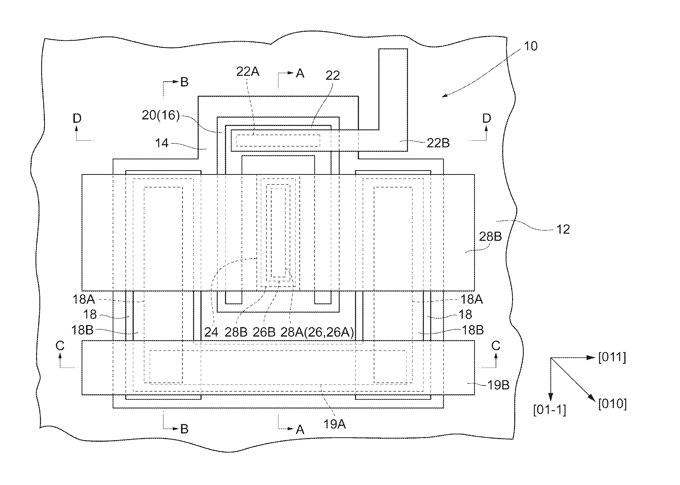
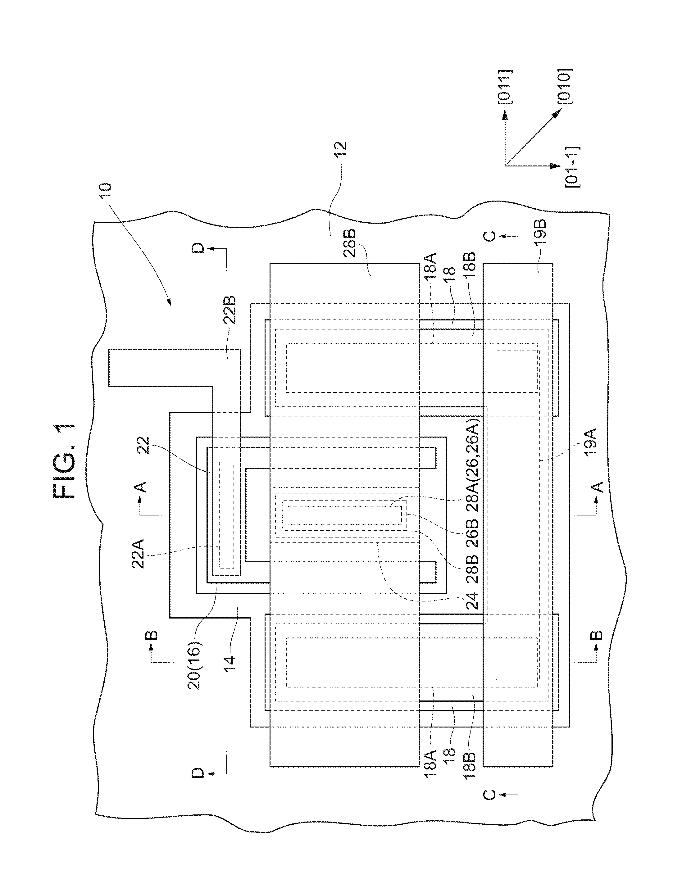
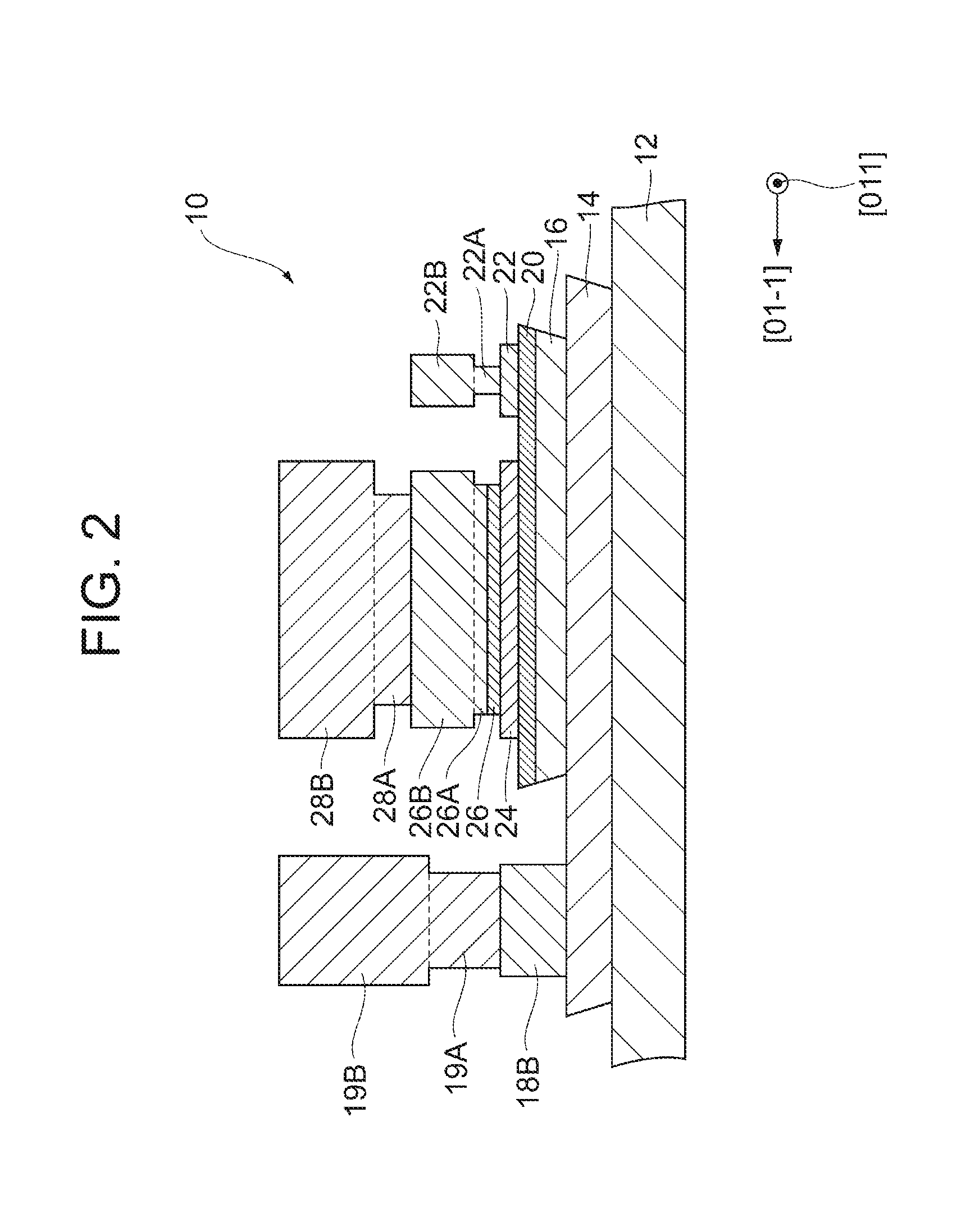
[0024]First, the structure of the HBT according to the first embodiment will be described below. FIG. 1 is a plan view of an HBT 10 as an example of the bipolar transistor according to the first embodiment of the present invention. FIG. 2 is a cross-sectional view taken along line A-A of FIG. 1. FIG. 3 is a cross-sectional view taken along line B-B of FIG. 1. FIG. 4 is a cross-sectional view taken along line C-C of FIG. 1. FIG. 5 is a cross-sectional view taken along line D-D of ...

second embodiment

[0077]An HBT according to a second embodiment of the present invention will be described below.

[0078]The HBT according to the second embodiment is different from the HBT according to the first embodiment, in a base line drawing method. The other configurations are the same as in the first embodiment.

[0079]FIG. 6 is a plan view of an HBT 40 as an example of a bipolar transistor according to the second embodiment of the present invention.

[0080]As illustrated in FIG. 6, the HBT 40 includes a base line 42 connected to a base electrode 22 via a contact hole 22A. The base line 42 is drawn out from an end in the short-side direction of the collector layer. As a result, the base line 42 goes over the side surfaces which are the forward mesa surfaces of the base layer 20, the collector layer 16, and the sub collector layer 14. More specifically, the base line 42 includes a first portion 42A, a second portion 42B, and a third portion 42C.

[0081]The first portion 42A is a portion that is presen...

third embodiment

[0085]A semiconductor device according to a third embodiment of the present invention will be described below.

[0086]FIG. 7 is a plan view of a semiconductor device 50 according to the third embodiment of the present invention.

[0087]The semiconductor device 50 according to the third embodiment includes at least one HBT 10 which has been described in the first embodiment and at least one HBT 60 different from the HBT 10 in the base line drawing method.

[0088]The HBT 60 includes a sub collector layer 62, a collector layer 64, a collector electrode 66, a base layer 68, a base electrode 70, an emitter layer 72, and an emitter electrode 74. The HBT 60 further includes a collector line 76, an emitter line 78, and a base line 80.

[0089]The collector layer 64 and the base layer 68 contain, for example, GaAs as a major component. The collector layer 64 and the base layer 68 have, for example, a rectangular shape. In the collector layer 64 and the base layer 68, the long-side direction thereof e...


PUM


Abstract

Disconnection of a base line is suppressed even when a short-side direction of a collector layer is parallel to crystal orientation [011]. A bipolar transistor includes: a collector layer that has a long-side direction and a short-side direction in a plan view, in which the short-side direction is parallel to crystal orientation [011], a cross-section perpendicular to the short-side direction has an inverted mesa shape, and a cross-section perpendicular to the long-side direction has a forward mesa shape; a base layer that is formed on the collector layer; a base electrode that is formed on the base layer; and a base line that is connected to the base electrode and that is drawn out from an end in the short-side direction of the collector layer to the outside of the collector layer in a plan view.

Description

BACKGROUND OF THE INVENTION[0001]1. Field of the Invention[0002]The present invention relates to a bipolar transistor, a semiconductor device, and a bipolar transistor manufacturing method.[0003]2. Background Art[0004]In the related art, development of a bipolar transistor having a collector layer, a base layer, and an emitter layer on a substrate has been attempted.[0005]Patent Document 1 discloses a bipolar transistor in which a base line connected to a base electrode coming into contact with a base layer is drawn out from an end in a long-side direction of a rectangular collector layer in a plan view.CITATION LISTPatent Document[0006][Patent Document 1] JP2004-327904 ASUMMARY OF THE INVENTION[0007]However, in the bipolar transistor described in Patent Document 1, since the collector layer is wet-etched, etching anisotropy may occur depending on crystal orientations of the collector layer. As a result, in the collector layer, a cross-section perpendicular to crystal orientation [0...

Claims


Application Information

Patent Timeline
Patent Type & Authority Applications(United States)
IPC IPC(8): H01L29/73H01L29/66
CPCH01L29/66234H01L29/73H01L23/4824H01L27/0605H01L29/0692H01L29/0821H01L29/66318H01L29/7371H01L29/205H01L2224/49171H01L2224/49111H01L2924/1305H01L2924/00H01L23/66H01L25/16H01L2223/6655H01L27/0823H01L23/535H01L25/0655H01L21/30612H01L29/045H01L29/1004H01L29/66242
Inventor SASAKI, KENJI
Owner MURATA MFG CO LTD
Why Eureka
Try Eureka