Metallic material for electronic components, and connector terminals, connectors and electronic components using same

a technology of electronic components and metal materials, applied in the direction of metallic pattern materials, metallic material coating processes, solid-state diffusion coatings, etc., to achieve the effects of low insertion/extraction force, high durability, and low degree of whisker formation

Active Publication Date: 2015-02-19
JX NIPPON MINING& METALS CORP
View PDF1 Cites 16 Cited by
  • Summary
  • Abstract
  • Description
  • Claims
  • Application Information

AI Technical Summary

Benefits of technology

[0046]According to the present invention, it is possible to provide a metallic material for electronic components having a low degree of insertion / extraction force, a low degree of whisker formation and a high durability, and connector terminals, connectors and electronic components using the metallic material.

Problems solved by technology

In the production process, on the plating surface, there occur sometimes whiskers, which are needle crystals, causing problems such as short circuiting, and hence such whiskers are also required to be suppressed satisfactorily.

Method used


Image

  • Metallic material for electronic components, and connector terminals, connectors and electronic components using same
  • Metallic material for electronic components, and connector terminals, connectors and electronic components using same
  • Metallic material for electronic components, and connector terminals, connectors and electronic components using same

Examples


examples

[0094]Hereinafter, Examples of the present invention are presented together with Comparative Examples; these Examples and Comparative Examples are provided for better understanding of the present invention, and are not intended to limit the present invention.

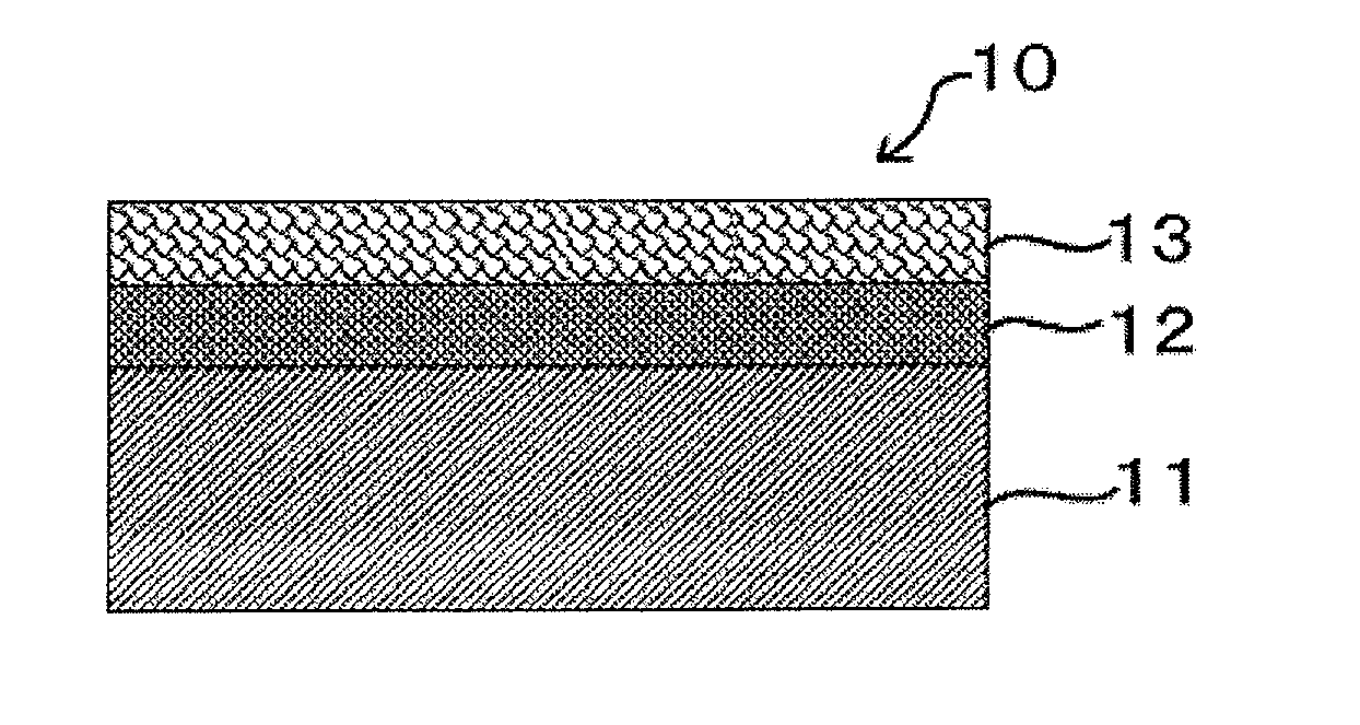
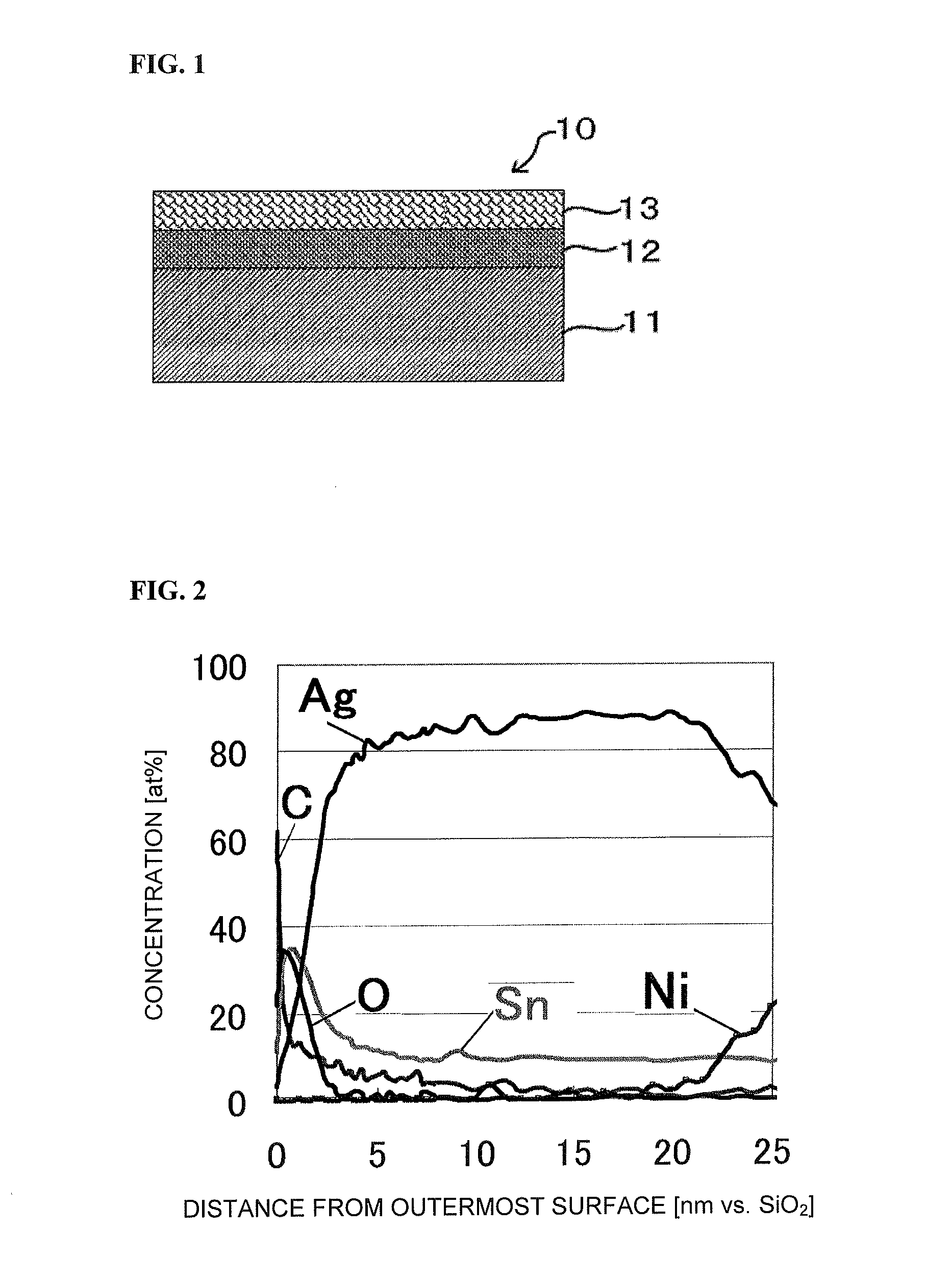
[0095]As Examples and Comparative Examples, the samples each formed by arranging a base material, a lower layer and an upper layer in this order and by heat treating the resulting arranged were prepared under the conditions shown in Tables 1 to 6 presented below.

[0096]Table 1 shows the preparation conditions of the base material, Table 2 shows the preparation conditions of the lower layer, Table 3 shows the preparation conditions of the upper layer and Table 4 shows the heat treatment conditions. Table 5 (Table 5-1, Table 5-2 and Table 5-3) shows the preparation conditions of the respective layers and the heat treatment conditions used in each of Examples, and Table 6 shows the preparation conditions of the respective layers and...


PUM

PropertyMeasurementUnit
thicknessaaaaaaaaaa
thicknessaaaaaaaaaa
thicknessaaaaaaaaaa

Abstract

The present invention provides a metallic material for electronic components having a low degree of whisker formation and a high durability, and connector terminals, connectors and electronic components using the metallic material. The metallic material for electronic components includes: a base material; on the base material, an lower layer constituted with one or two or more selected from the group consisting of Ni, Cr, Mn, Fe, Co and Cu; on the lower layer, an upper layer constituted with an alloy composed of one or both of Sn and In (constituent elements A) and one or two or more of Ag, Au, Pt, Pd, Ru, Rh, Os and Ir (constituent elements B), wherein the thickness of the lower layer is 0.05 μm or more; the thickness of the upper layer is 0.005 μm or more and 0.6 μm or less; and in the upper layer, the relation between the ratio, the constituent elements A/(the constituent elements A+the constituent elements B) [mass %] (hereinafter, referred to as the proportion of Sn+In) and the plating thickness [μm] is given by
plating thickness≦8.2×(proportion of Sn+In)−0.66 [herein, (the proportion of Sn+In)≧10 mass %].

Description

TECHNICAL FIELD[0001]The present invention relates to a metallic material for electronic components, and connector terminals, connectors and electronic components using the same.BACKGROUND ART[0002]In connectors as connecting components for electronic devices for consumer use and for vehicle use, materials are used in which base plating of Ni or Cu is applied to the surface of brass or phosphor bronze materials and Sn or Sn alloy plating is further applied to the base plating. Sn or Sn alloy plating is generally required to have properties such as low contact resistance and high solder wettability, and further, recently the reduction of the insertion force has also been required at the time of joining together a male terminal and a female terminal molded by press processing of plating materials. In the production process, on the plating surface, there occur sometimes whiskers, which are needle crystals, causing problems such as short circuiting, and hence such whiskers are also requ...

Claims


Application Information

Patent Timeline
Patent Type & Authority Applications(United States)
IPC IPC(8): H01B1/02B32B15/01H01R4/58
CPCH01B1/02B32B15/01H01R4/58B32B15/018C22C5/04C22C5/06C22C13/00C22C19/03C23C10/28C23C10/60C23C14/14C23C14/58C23C28/021H01R13/03H05K1/09H05K3/244Y10T428/12681Y10T428/12708Y10T428/12715Y10T428/12722
Inventor SHIBUYA, YOSHITAKAFUKAMACHI, KAZUHIKOKODAMA, ATSUSHI
Owner JX NIPPON MINING& METALS CORP
Why Eureka
Try Eureka