Nitride semiconductor element and method for producing same

a semiconductor element and nitride technology, applied in semiconductor/solid-state device manufacturing, semiconductor devices, electrical equipment, etc., can solve the problems of increased production cost, deterioration, and inability to perform wire bonding, so as to minimize contact resistance, reduce production cost, and increase production. the effect of the number of producing steps

Active Publication Date: 2015-02-19
NIKKISO COMPANY
View PDF2 Cites 23 Cited by
  • Summary
  • Abstract
  • Description
  • Claims
  • Application Information

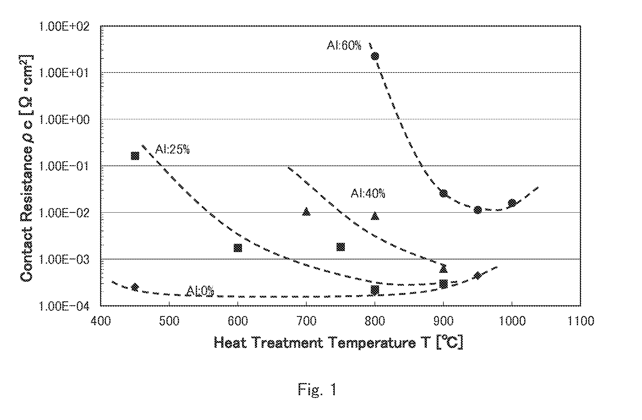
AI Technical Summary

Benefits of technology

[0017]As described above, in the case of the ultraviolet light emitting element having the emission wavelength of 365 nm or less, the heat treatment at 600° C. or more is needed for the n-electrode. The above method for forming the electrode, in which after the n-electrode and the p-electrode are subjected to the heat treatment, the Au layer is formed again on each electrode and the heat treatment is not performed after that is the most reliable solution, but in this method, the number of steps of forming the electrode is increased, and Au consumption is increased, so that the problem is that the production cost becomes high.
[0030]In addition, it is more preferable that a process temperature of the second annealing process is lower than a process temperature of the first annealing process, in the method for producing the nitride semiconductor element having the above characteristics. With this configuration, the influence by the second annealing process is prevented, and the first annealing process can be performed at an optimal temperature based on the AlN mole fraction of the n-type AlGaN based semiconductor layer to minimize the contact resistance between the n-electrode contact part and the n-type AlGaN based semiconductor layer.

Problems solved by technology
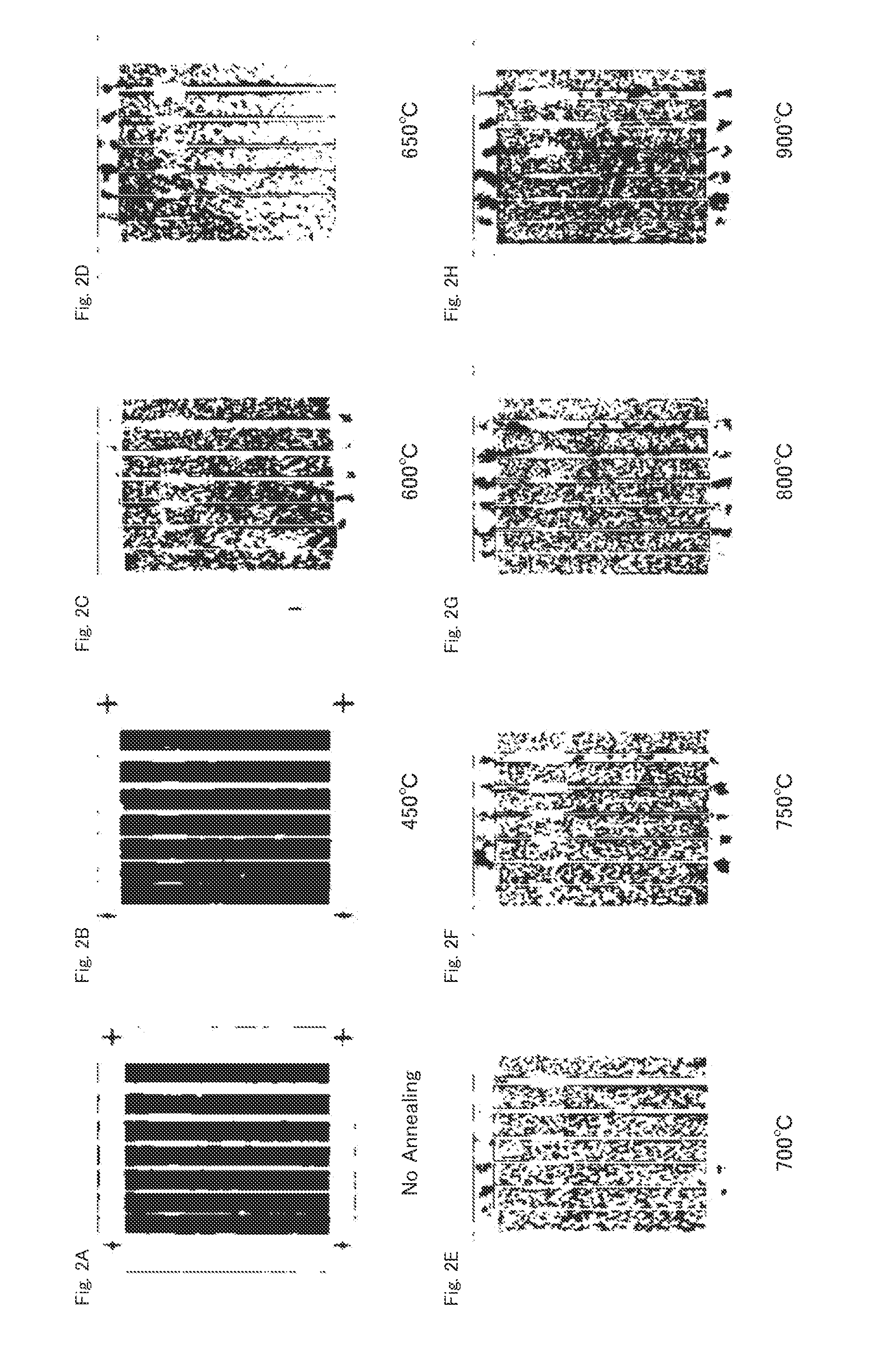
However, due to the heat treatment, the metal layer on the lower layer side is alloyed with Au on the upper layer side, and the alloyed metal other than Au is exposed to a surface of each electrode and deteriorates a surface state, so that the wire bonding cannot be performed in some cases, and the deterioration becomes noticeable especially in a case where a heat treatment temperature is high.
However, this countermeasure has the problem that production cost is increased because the number of the film forming steps is increased.

Method used


Image

  • Nitride semiconductor element and method for producing same
  • Nitride semiconductor element and method for producing same
  • Nitride semiconductor element and method for producing same

Examples


Embodiment Construction

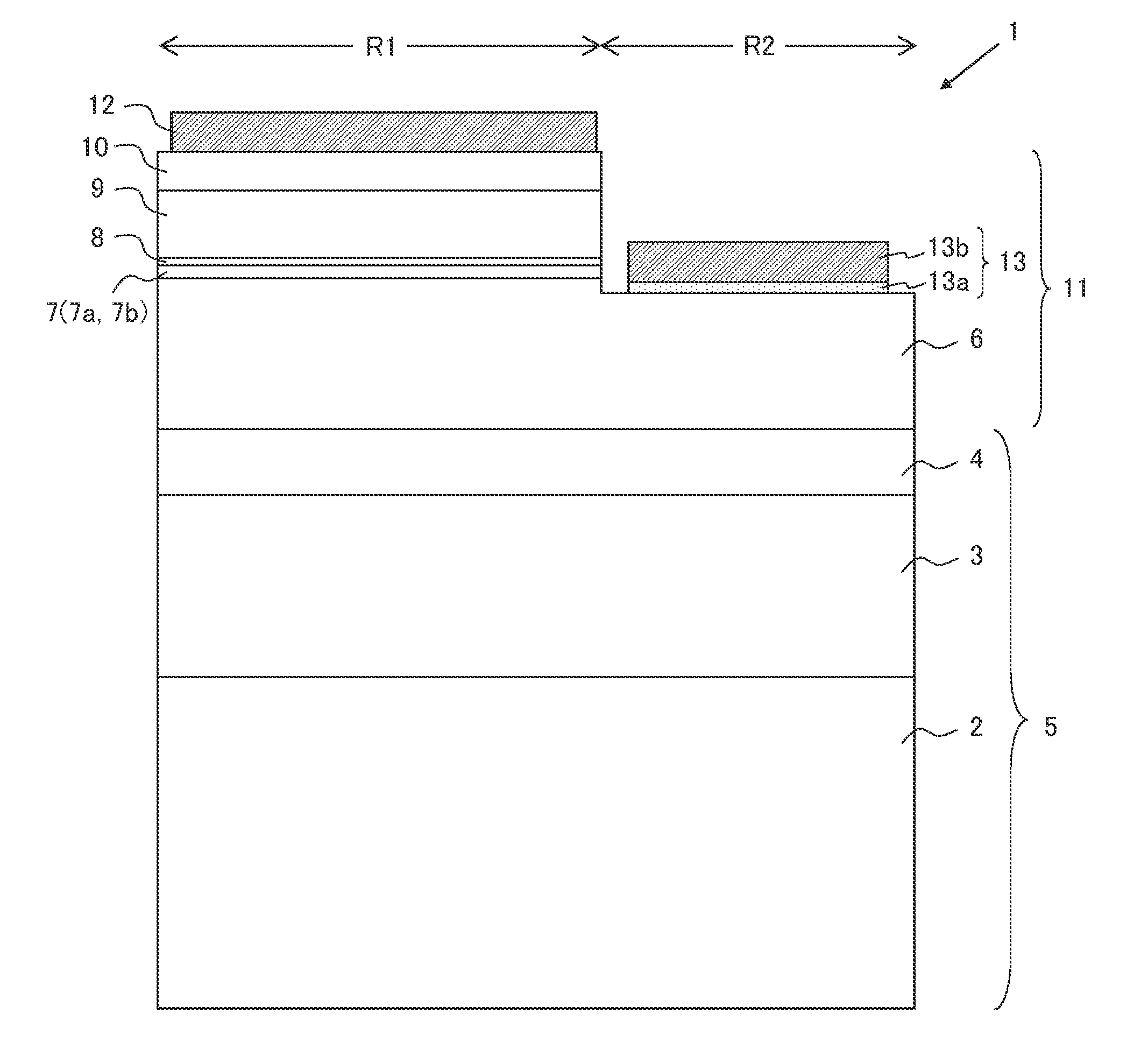
[0043]An embodiment of a nitride semiconductor element according to the present invention will be described with reference to the drawings. In addition, in the drawings used in the following description, a substantial part is emphasized to schematically describe the contents of the present invention for ease in understanding the description, so that a dimension ratio of each part is not always the same as a dimension ratio of an actual element. Hereinafter, this embodiment will be described assuming that the nitride semiconductor element according to the present invention is an ultraviolet light emitting element, and furthermore the nitride semiconductor element is a light emitting diode. In the following description, the nitride semiconductor element according to the present invention is simply referred to as “light emitting element”.

[0044]As shown in FIG. 4, a light emitting element 1 according to this embodiment has a laminated structure in which a substrate is used as a template...


PUM

PropertyMeasurementUnit
mole fractionaaaaaaaaaa
temperatureaaaaaaaaaa

Abstract

A nitride semiconductor element 1 includes a base structure part 5, and an element structure part 11 formed on the base structure part 5 and having at least an n-type AlGaN based semiconductor layer 6, and p-type AlGaN based semiconductor layers 8, 9, 10, and further includes an n-electrode contact part 13a formed on the n-type AlGaN based semiconductor layer 6, an n-electrode pad part 13b formed on the n-electrode contact part 13a, and a p-electrode 12 formed on the p-type AlGaN based semiconductor layers 8, 9, 10, in which an AlN mole fraction in the n-type AlGaN based semiconductor layer 6 is 20% or more, the n-electrode contact part 13a includes one or more metal layers, and the p-electrode 12 and the n-electrode pad part 13b have a common laminated structure of two or more layers having an Au layer as an uppermost layer, and an Au diffusion preventing layer composed of conductive metal oxide and formed under the uppermost layer to prevent Au diffusion.

Description

CROSS-REFERENCE TO RELATED APPLICATIONS[0001]This application is a National Phase filing under 35 U.S.C. §371 of International Application No. PCT / JP2011 / 072524 filed on Sep. 30, 2011.TECHNICAL FIELD[0002]The present invention relates to a nitride semiconductor element and a method for producing the same, particularly relates to a nitride semiconductor element having a light emission center wavelength of about 365 nm or less used in a light emitting diode or a laser diode and a method for producing the same, and more specifically relates to an electrode structure of an n-electrode and a p-electrode used in the element.BACKGROUND ART[0003]Conventionally, a nitride semiconductor light emitting element such as a light emitting diode (LED) or a semiconductor laser has a light emitting element structure in which a plurality of nitride semiconductor layers are epitaxially grown on a sapphire substrate in many cases. The nitride semiconductor layer is expressed by a general formula: Al1-x-...

Claims


Application Information

Patent Timeline
Patent Type & Authority Applications(United States)
IPC IPC(8): H01L33/00H01L33/62H01L33/40H01L33/32H01L33/06H01L33/38
CPCH01L33/0095H01L33/06H01L33/0075H01L33/387H01L2933/0066H01L33/32H01L33/62H01L2933/0016H01L33/40H01L29/2003H01L29/452H01L33/382H01L33/405
Inventor NIWA, NORITAKAINAZU, TETSUHIKO
Owner NIKKISO COMPANY
Why Eureka
Try Eureka