Tungsten deposition with tungsten hexafluoride (WF6) etchback

a technology of tungsten hexafluoride and etchback, which is applied in the direction of coating, chemical vapor deposition coating, metallic material coating process, etc., can solve the problems of increased processing capacity, improper operation, and increased difficulty in this process

Active Publication Date: 2015-02-19
APPLIED MATERIALS INC
View PDF2 Cites 86 Cited by
  • Summary
  • Abstract
  • Description
  • Claims
  • Application Information

AI Technical Summary

Benefits of technology

[0010]Implementations described herein generally relate to the processing of substrates, and more particularly relate to methods for forming tungsten materials on substrates using vapor deposition processes. In one implementation a method for depositing a tungsten film on a substrate is provided. The method comprises positioning a substrate having a feature formed therein in a substrate processing chamber, wherein the feature is defined by at least one sidewall and a bottom surface, depositing a first film of a bulk tungsten layer by introducing a continuous flow of a hydrogen containing gas and a tungsten halide compound to the processing chamber to deposit the first tungsten film over the feature, etching the first film of the bulk tungsten layer using a plasma treatment to remove a portion of the first film by exposing the first film to a continuous flow of the tungsten halide compound and an activated treatment gas and depositing a second film of the bulk tungsten layer by introducing a continuous flow of the hydrogen containing gas and the tungsten halide compound to the processing chamber to deposit the second tungsten film over the first tungsten film.

Problems solved by technology

The shrinking dimensions of circuits and devices have placed additional demands on processing capabilities.
But successive reduction in feature sizes has meant that there is increasing difficulty in this process.
The presence of the void 30 changes the material and operating characteristics of the interconnect feature and may eventually cause improper operation and premature breakdown of the device.

Method used


Image

  • Tungsten deposition with tungsten hexafluoride (WF6) etchback
  • Tungsten deposition with tungsten hexafluoride (WF6) etchback
  • Tungsten deposition with tungsten hexafluoride (WF6) etchback

Examples


Embodiment Construction

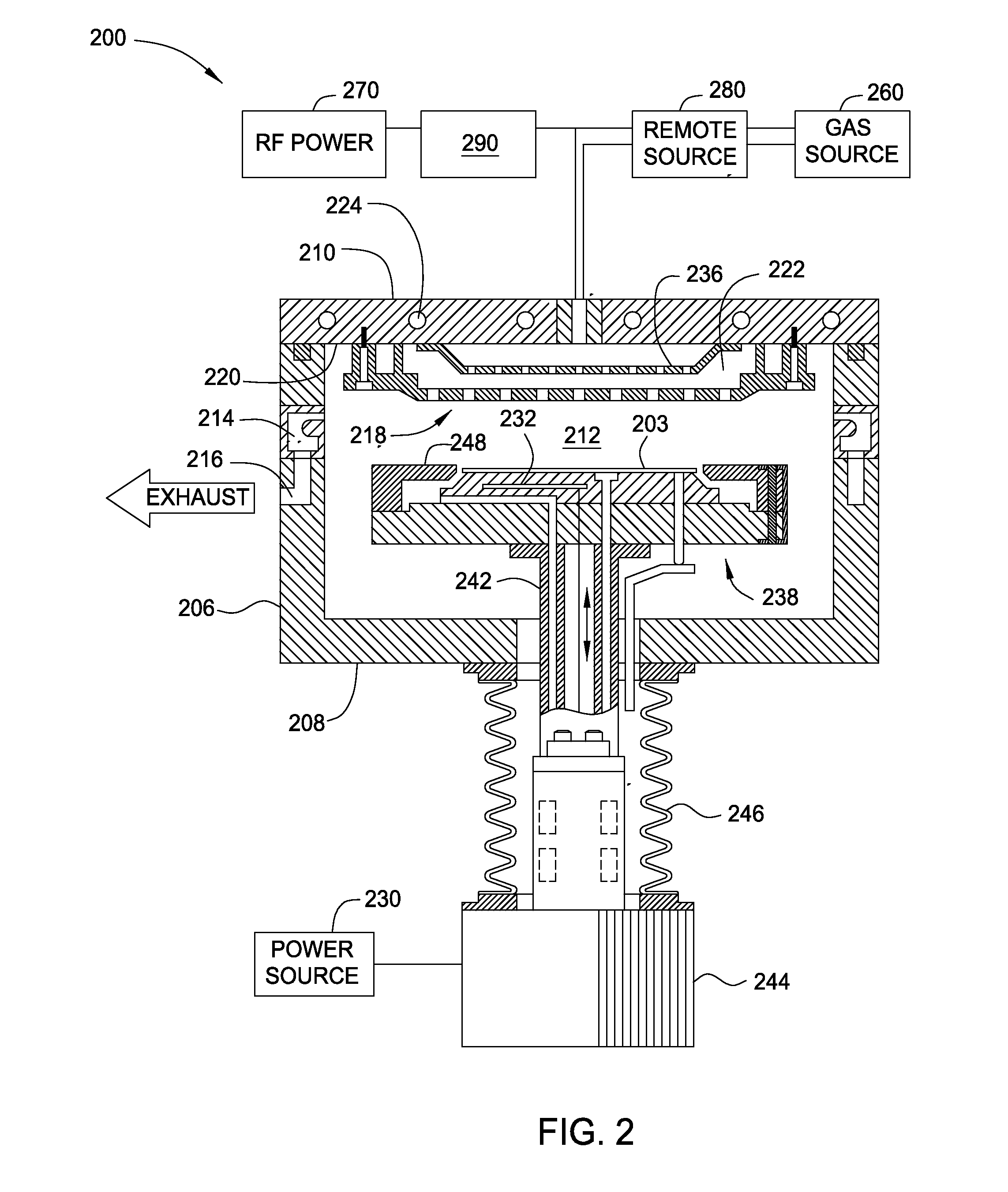
[0018]Implementations described herein generally relate to the processing of substrates, and more particularly relate to methods for forming tungsten materials on substrates using vapor deposition processes.

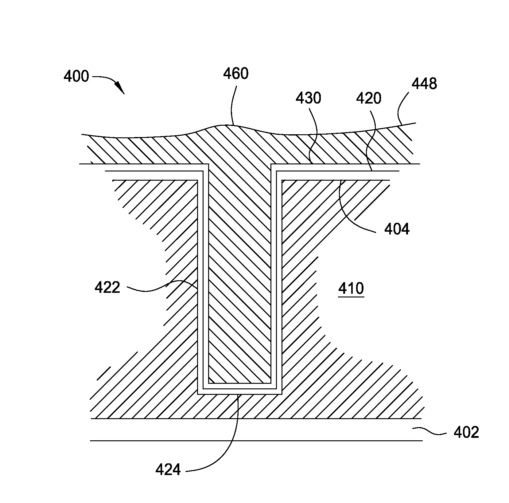
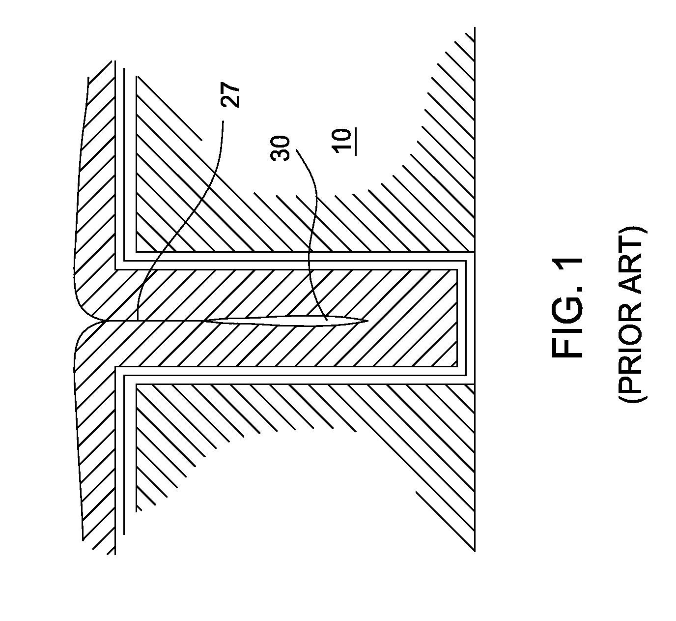
[0019]Tungsten (W) has been used at contact level in logic application for about two decades. In recent advanced CMOS devices, new technology such as metal gate and FinFET emerge, which leads to a new application for tungsten as metal gate fill for both PMOS and NMOS devices. In 3D NAND devices, tungsten is also used for metal gate fill. The requirements for tungsten fill become more and more challenging. For contact, the overhang becomes more challenging as the dimensions of contacts are getting smaller and typically leaves a big seam after tungsten conformal fill. Furthermore, the seam will be exposed to slurry during WCMP, which causes integration issues. For metal gate trench in both advanced CMOS and 3D NAND, traditional tungsten conformal growth inevitably leaves a seam in ...


PUM

PropertyMeasurementUnit
thicknessaaaaaaaaaa
thicknessaaaaaaaaaa
thicknessaaaaaaaaaa

Abstract

Implementations described herein generally relate to methods for forming tungsten materials on substrates using vapor deposition processes. The method comprises positioning a substrate having a feature formed therein in a substrate processing chamber, depositing a first film of a bulk tungsten layer by introducing a continuous flow of a hydrogen containing gas and a tungsten halide compound to the processing chamber to deposit the first tungsten film over the feature, etching the first film of the bulk tungsten layer using a plasma treatment to remove a portion of the first film by exposing the first film to a continuous flow of the tungsten halide compound and an activated treatment gas and depositing a second film of the bulk tungsten layer by introducing a continuous flow of the hydrogen containing gas and the tungsten halide compound to the processing chamber to deposit the second tungsten film over the first tungsten film.

Description

CROSS-REFERENCE TO RELATED APPLICATIONS[0001]This application claims benefit of U.S. provisional patent application Ser. No. 61 / 866,665, filed Aug. 16, 2013. The aforementioned related patent application is herein incorporated by reference in its entirety,BACKGROUND[0002]1. Field[0003]Implementations described herein generally relate to the processing of substrates, and more particularly relate to methods for forming tungsten materials on substrates using vapor deposition processes.[0004]2. Description of the Related Art[0005]Reliably producing nanometer-sized features is one of the key technologies for the next generation of semiconductor devices. The shrinking dimensions of circuits and devices have placed additional demands on processing capabilities. The multilevel interconnects that lie at the heart of integrated circuit technology require precise processing of high aspect ratio features, such as vies and other interconnects. Reliable formation of these interconnects is very im...

Claims


Application Information

Patent Timeline
Patent Type & Authority Applications(United States)
IPC IPC(8): H01L21/3205H01L21/3213
CPCH01L21/32136H01L21/32051C23C16/045C23C16/14H01L21/28556H01L21/76877
Inventor WU, KAIYU, SANG HO
Owner APPLIED MATERIALS INC
Why Eureka
Try Eureka