Vertical Light Emitting Device and Manufacturing Method Thereof

a technology of light emitting device and manufacturing method, which is applied in the manufacture of semiconductor/solid-state devices, semiconductor devices, electrical devices, etc., can solve the problems of lateral structure that cannot be driven by high current density, and achieve low luminous efficiency and high thermal resistance

Active Publication Date: 2015-03-05
XIAMEN SANAN OPTOELECTRONICS TECH CO LTD
View PDF0 Cites 17 Cited by
  • Summary
  • Abstract
  • Description
  • Claims
  • Application Information

AI Technical Summary

Benefits of technology

[0006]The present invention relates to a vertical HV luminous element and fabrication method thereof, which achieves polarity reversal of two adjacent LEDs via regional laser stripping and die bonding. The two polarity-reversed LEDs are placed on an insulating substrate containing metal bonding wires; and wires are made on the surfaces of the luminous elements to make the single LED cell as vertical structure and a plurality LED cascaded into HV LED, thus overcoming the problems of low luminous efficiency and high thermal resistance of the traditional lateral structure.

Problems solved by technology

Traditional DC LED elements need to use power converters such as switch power to convert the commercial power supply into low-voltage power, which causes loss during this process.
FIG. 1 is the sectional structural view of a lateral HV LED, which reduces power loss at the power conversion end; however, the single LED unit 110 has a lateral structure that cannot be driven by high current density owing to low luminous efficiency, current blockage, high thermal resistance, etc., of lateral LED chips.

Method used


Image

  • Vertical Light Emitting Device and Manufacturing Method Thereof
  • Vertical Light Emitting Device and Manufacturing Method Thereof
  • Vertical Light Emitting Device and Manufacturing Method Thereof

Examples


embodiment 1

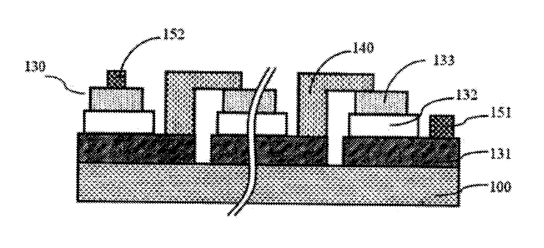
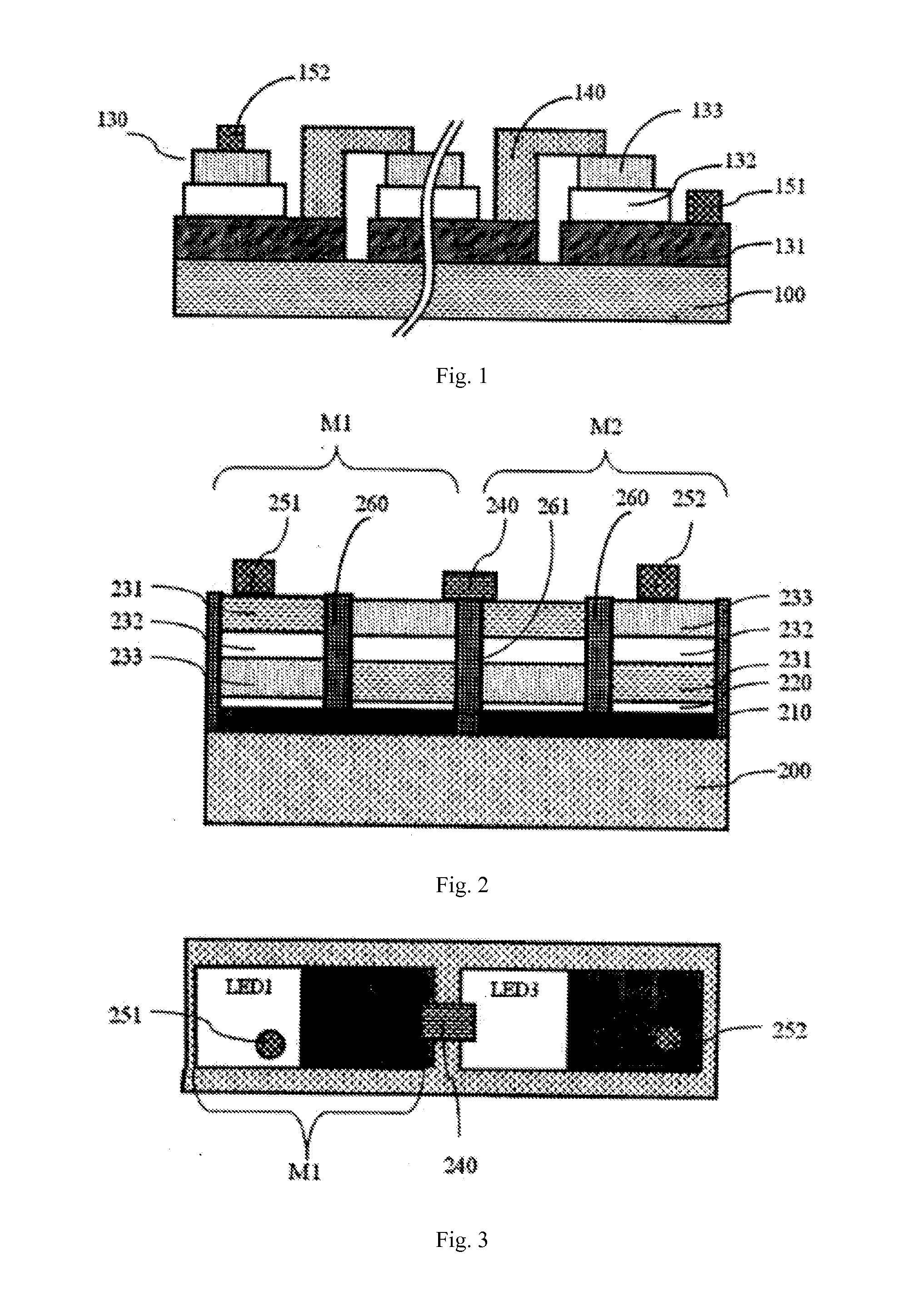
[0036]FIG. 21 is a top view of the vertical DC HV luminous element according to the present invention. As shown in FIG. 21, fabricate metal wires at 7 connection points between “LED2 and LED3, LED4 and LED8, LED7 and LED6, LEDS and LED9, LED10 and LED11, LED12 and LED16, LED15 and LED14” to form the conductive structure 440. Fabricate the first electrode 451 on LED1 and the second electrode 452 on LED13. The 16-series vertical DC HV LED luminous element is fabricated. Refer to FIG. 22 for the circuit diagram.

embodiment 2

[0037]FIG. 23 is a top view of vertical AC HV luminous element according to the present invention. As shown in FIG. 23, fabricate metal wires at 6 connection points between “LED1 and LEDS, LED4 and LED8, LED6 and LED10, LED7 and LED11, LED9 and LED13, LED12 and LED16” to form the conductive structure 540. Fabricate the first electrode 551 between LED2 and LED3, which connects the p-GaN layer of LED2 and the n-GaN layer of LED3; and fabricate the second electrode 552 between LED14 and LED15, which connects the n-GaN layer of LED14 and the p-GaN layer of LED15. The vertical AC HV LED luminous element is fabricated. Refer to FIG. 24 for the circuit diagram. The flow of the first LED circuit current is: A-LED14-LED13-LED9-LED10-LED6-LEDS-LED1-LED2-B; and the flow of the second circuit current is B-LED3-LED4-LED8-LED7-LED11-LED12-LED16-LED15-B.


PUM


Abstract

A vertical high-voltage light emitting device and a manufacturing method thereof. Polarities of two adjacent light emitting diodes (LEDs) are reversed by means of area laser stripping and die bonding, and the two diodes whose polarities are reversed are disposed on an insulating substrate comprising a bonding metal layer (320). A conductive wire (140) is distributed on a surface of the light emitting device, so that a single LED unit (330) has a vertical structure, and multiple LEDs are connected in series to form a high-voltage LED, thereby solving the problems of low light emitting efficiency and large thermal resistance of a horizontal structure.

Description

[0001]This application claims priority to the Chinese Patent Application No. 201210130389.2 entitled “Vertical Light Emitting Device and Manufacturing Method Thereof” and filed with the Chinese Patent Office on Apr. 28, 2012, which is hereby incorporated by reference in its entirety.FIELD OF THE INVENTION[0002]The present invention relates to a semiconductor luminous element and fabrication method thereof, and more particularly, to a vertical HV luminous element and fabrication method thereof.BACKGROUND OF THE INVENTION[0003]The LED of solid luminous elements, owing to electrical and optical advantages such as low energy consumption, long service life, good stability, small size, fast response and stable luminous wave length, is widely applied in fields like illumination, household appliance, display and indicator. Moreover, this kind of luminous elements enjoys considerable progress in luminous effect and service life and therefore, is promising to become the mainstream for a new g...

Claims


Application Information

Patent Timeline
Patent Type & Authority Applications(United States)
IPC IPC(8): H01L33/62H01L33/20
CPCH01L33/62H01L2933/0033H01L33/20H01L25/0753H01L33/44H01L2924/0002
Inventor ZENG, XIAOQIANGCHEN, SHUNPINGHUANG, SHAOHUAPAN, QUNFENGWU, JYH-CHIARNG
Owner XIAMEN SANAN OPTOELECTRONICS TECH CO LTD
Why Eureka
Try Eureka