

Compound semiconductor structure
a semiconductor and compound technology, applied in the field of semiconductor structure, can solve the problems of large lattice mismatch between crystalline silicon substrate and compound semiconductor crystal, low charge carrier mobility, and limited use of silicon in particular in opto-electronic applications
- Summary
- Abstract
- Description
- Claims
- Application Information
AI Technical Summary
Benefits of technology
Problems solved by technology
Method used
Image

Examples
Embodiment Construction
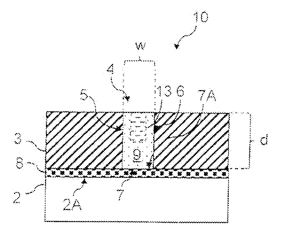
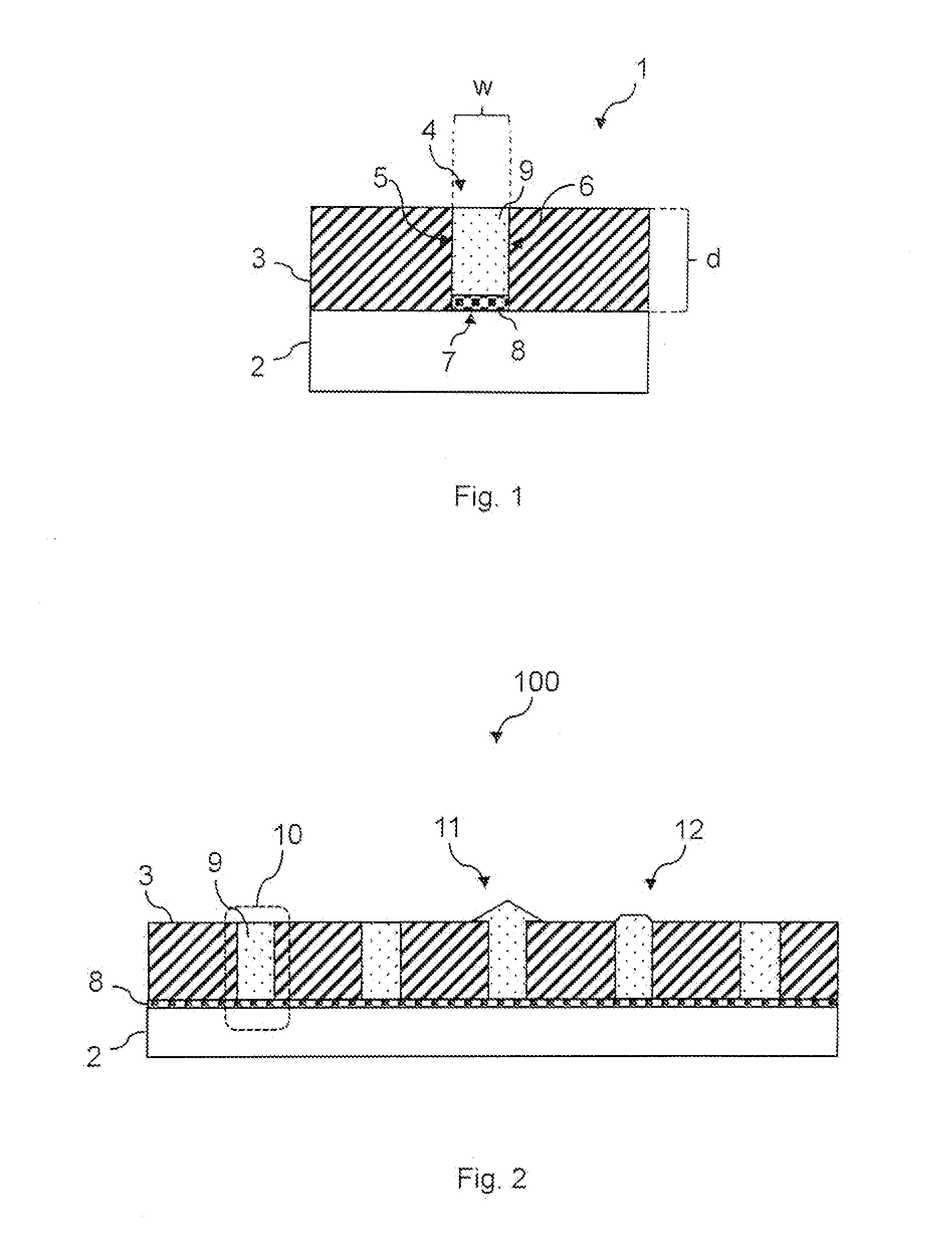
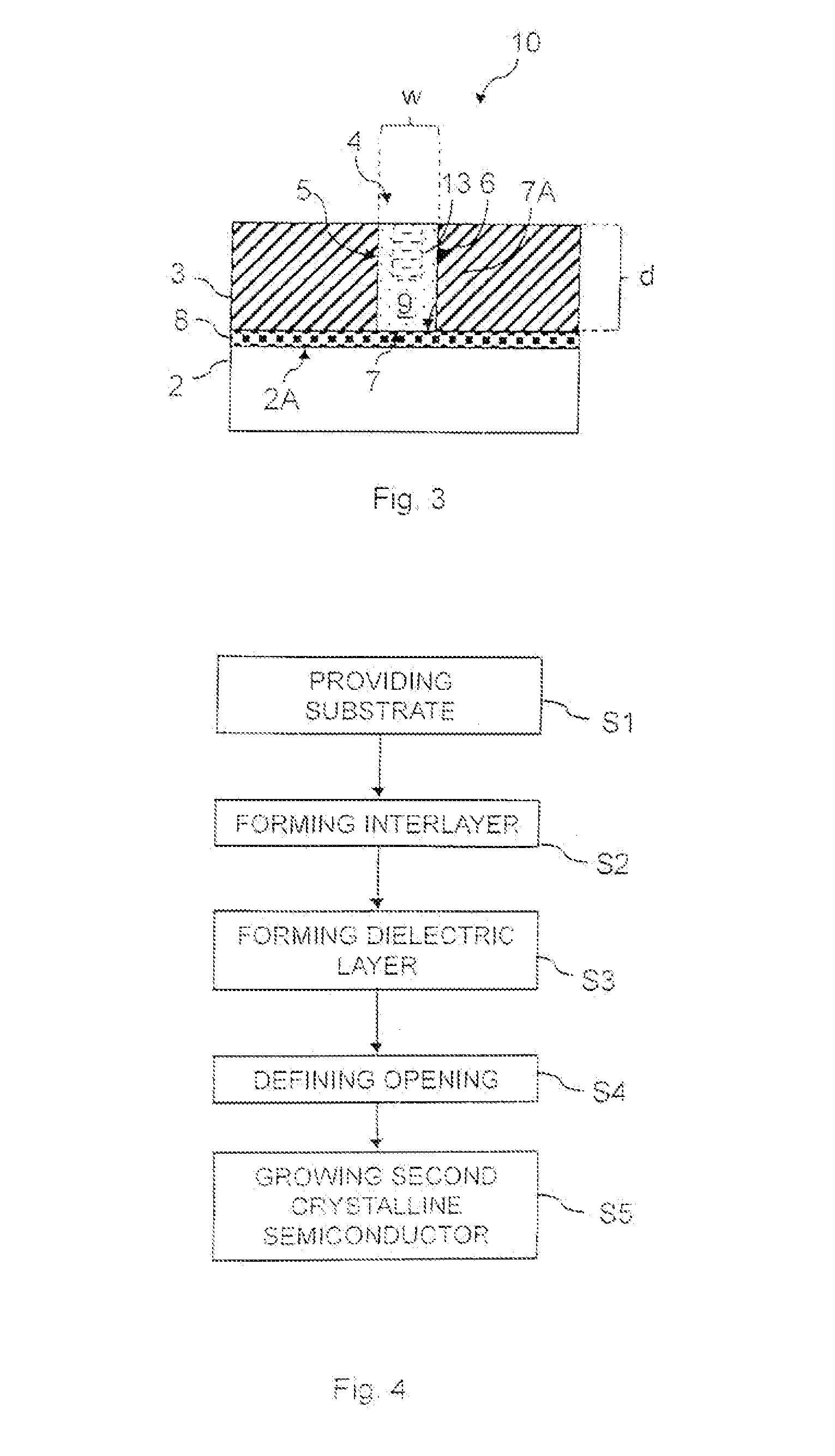
[0014]Silicon is the basic material for present solid-state electronics, and processing techniques have been evolved for decennials. Hence, most electronic integrated circuit devices are based on silicon. However, the relatively low charge carrier mobility and its indirect band gap are disadvantages and limit the use of silicon in particular in opto-electronic applications. It would be advantageous to combine more suitable semiconductor materials, such as III-V or IV-IV compound semiconductors, with silicon-based electronics on common silicon substrates.
[0015]It is, therefore, desirable to provide improved devices comprising lattice mismatched crystalline semiconductor materials and methods for fabricating such.
[0016]It is an aspect of the present disclosure to provide improved semiconductor structures based on a crystalline semiconductor material grown on a crystalline semiconductor substrate wherein the semiconductor material and the substrate semiconductor material have a lattice...
PUM
| Property | Measurement | Unit |
|---|---|---|
| aspect ratio | aaaaa | aaaaa |
| thickness | aaaaa | aaaaa |
| thickness | aaaaa | aaaaa |
Abstract
Description
Claims
Application Information