Method for Laterally Trimming a Hardmask

a technology of hardmask and cd, which is applied in the direction of basic electric elements, semiconductor/solid-state device manufacturing, electric devices, etc., can solve the problems of significant loss, unusable corresponding substrates (wafers), and large loss of hardmask cds, so as to prevent wafers from becoming unusable, precise lateral etching of the structure, and reduce the effect of critical dimension or dimension

Active Publication Date: 2015-03-05
TOKYO ELECTRON LTD
View PDF6 Cites 111 Cited by
  • Summary
  • Abstract
  • Description
  • Claims
  • Application Information

AI Technical Summary

Benefits of technology

[0004]Techniques herein provide a method to correct or tune CDs on a hardmask that do not meet a specified value. Techniques herein provide a method to shrink hardmask dimensions to prevent wafers from becoming unusable. Specifically, techniques herein provide a method of laterally etching a dielectric hardmask to fall within a specified CD to be viable for continued fabrication. Techniques include changing the chemistry in the breakthrough or main etch to tune the CD. This can trim a substantial portion of the dielectric hardmask, such as up to 6 nm or more. For example, this technique can reduce a critical dimension or dimension of a structure from about 36 nm to about 30 nm.
[0005]Changing carbon to fluorine (C / F) atomic ratio in processing plasmas enables protective polymer thickness control on dielectric mask sidewalls. Controlling this ratio makes possible precise lateral etching of the structure, i.e. “trimming” of the incoming mask. The C / F ratio in the plasma can be controlled by adjusting flow rates of two or several precursors with different C:F ratios in a molecular structure.
[0006]One benefit of methods herein is that the outgoing critical dimension (CD) can be controlled independently with no need for adjustment in lithography and Hard Mask Opening (HMO) processes. Features herein can significantly simplify the process optimization and reduce process development time.
[0007]Methods herein include a new etching scheme for “dielectric-Si” stack etching that includes a mask trimming step as part of the Si etching process. Thus, techniques herein can provide an all-in-one solution. Using a fluorocarbon mixture for dielectric mask trimming provides several advantages, such as it is straightforward to apply and gives additional flexibility to the process flow. Without the hardmask trim method disclosed herein, if a hardmask CD is not on target, then a wafer is scrapped. With hard-mask trim capability in silicon etch as disclosed herein, then a given CD can be re-targeted to eliminate wafer-scraps. For example, if a hardmask open process tool can only make a good profile for a particular CD identified as being wide (too wide), then this wide CD can be narrowed by executing techniques herein.

Problems solved by technology

If a given resulting hardmask has lines or features with a critical dimension (CD) that is too large, then corresponding substrates (wafers) are unusable and typically scrapped.
Such a wafer loss resulting from hardmask CDs that are too large can be a significant loss.

Method used


Image

  • Method for Laterally Trimming a Hardmask
  • Method for Laterally Trimming a Hardmask
  • Method for Laterally Trimming a Hardmask

Examples


Embodiment Construction

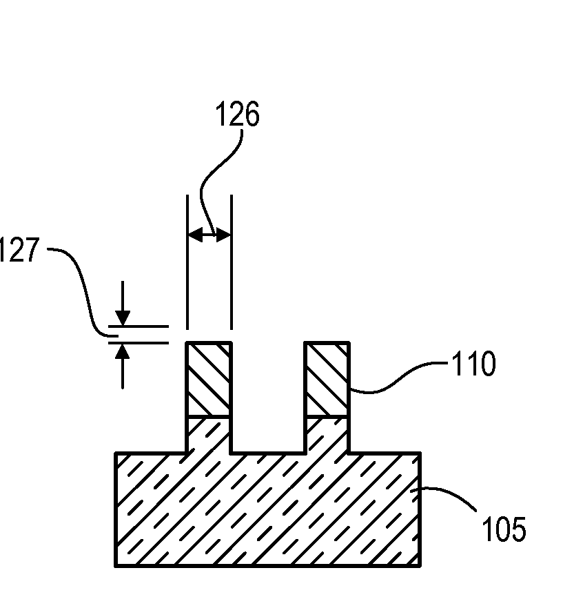
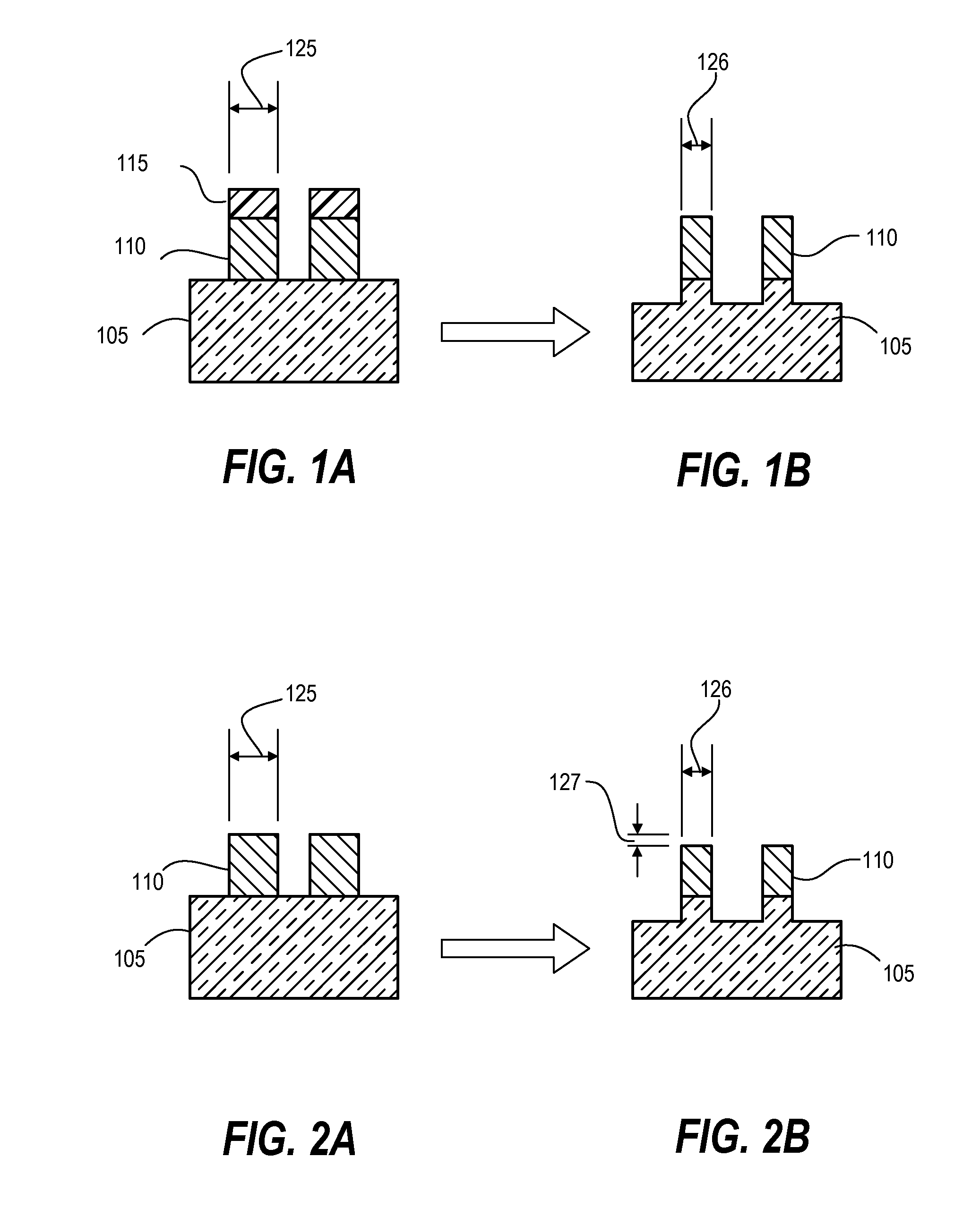
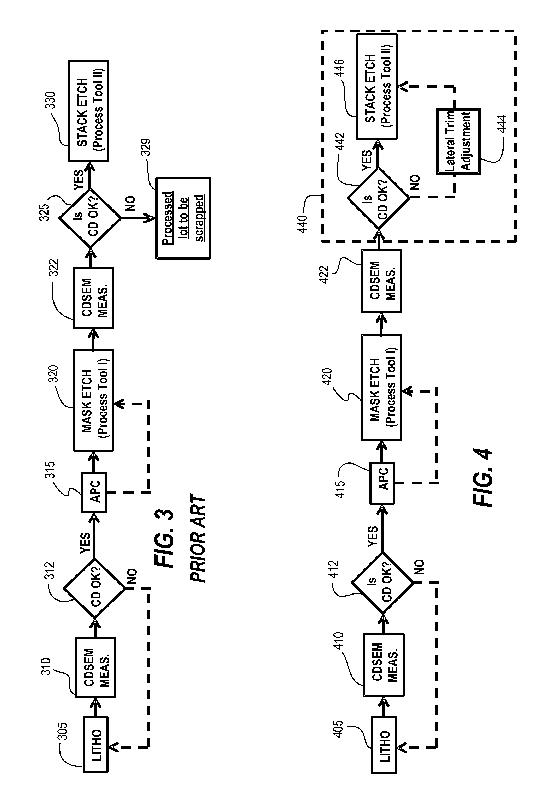
[0018]Techniques herein include methods of controllable lateral etching of dielectrics in polymerizing fluorocarbon plasmas. Methods herein include an etching scheme for “dielectric-Si” stack etching that includes a mask trimming step as part of the Si etching process. Thus, techniques herein can provide an all-in-one solution. Using a fluorocarbon mixture for dielectric mask trimming provides several advantages, such as it is straightforward to apply and gives additional flexibility to the process flow. Without the hardmask trim method disclosed herein, if a hardmask CD is not on target, then a wafer is scrapped. With hard-mask trim capability in silicon etch as disclosed herein, a given CD can be re-targeted to eliminate wafer-scraps. For example, if a hardmask open process tool can only make a good profile for a particular CD identified as being wide (too wide), then this wide CD can be narrowed by executing techniques herein.

[0019]Techniques herein provide a method to correct or...


PUM

PropertyMeasurementUnit
feature thicknessaaaaaaaaaa
thicknessaaaaaaaaaa
thicknessaaaaaaaaaa

Abstract

Techniques herein include methods for controllable lateral etching of dielectrics in polymerizing fluorocarbon plasmas. Methods can include dielectric stack etching that uses a mask trimming step as part of a silicon etching process. Using a fluorocarbon mixture for dielectric mask trimming provides several advantages, such as being straightforward to apply and providing additional flexibility to the process flow. Thus, techniques herein provide a method to correct or tune CDs on a hardmask. In general, this technique can include using a fluorine-based and a fluorocarbon-based, or fluorohydrocarbon-based, chemistry for creating a plasma, and controlling a ratio of the two chemistries. Without the hardmask trim method disclosed herein, if a hardmask CD is not on target, then a wafer is scrapped. With hard-mask trim capability in silicon etch as disclosed herein, a given CD can be re-targeted to eliminate wafer-scraps.

Description

CROSS REFERENCE TO RELATED APPLICATIONS[0001]The present application claims the benefit of U.S. Provisional Patent Application No. 61 / 870,546, filed on Aug. 27, 2013, entitled “Method for Laterally Trimming a Hardmask,” which is incorporated herein by reference in its entirety.BACKGROUND OF THE INVENTION[0002]This invention relates to plasma processing and, in particular, to etching of substrates using plasma products.SUMMARY[0003]Semiconductor fabrication involves creating a pattern of features in a substrate. This pattern is typically created using photolithography techniques. Photolithography techniques involve creating a latent pattern in photoresist, developing the latent pattern into a relief pattern, and then transferring the relief pattern into one or more underlying layers such as to create a hardmask, dielectric mask, or various structures that may be permanent or sacrificial. Transferring the relief pattern into underlying layers can be accomplished by etching techniques....

Claims


Application Information

Patent Timeline
Patent Type & Authority Applications(United States)
IPC IPC(8): H01L21/3065
CPCH01L21/3065H01L21/3086H01L21/31116H01L21/30604H01L21/308
Inventor RANJAN, ALOKVORONIN, SERGEY
Owner TOKYO ELECTRON LTD
Why Eureka
Try Eureka