Automatic retest method for system-level IC test equipment and IC test equipment using same

a technology of ic test equipment and retest method, which is applied in the direction of resistance/reactance/impedence, testing circuit, instruments, etc., can solve the problems of failure of semiconductor chips, failure of semiconductor chips having unsatisfactory performance, and failure of semiconductor chips with unsatisfactory performance, so as to reduce the possibility of misclassification, increase the efficiency of retest operation, and achieve reasonable and objective test results.

Inactive Publication Date: 2015-03-05
CHROMA ATE
View PDF35 Cites 3 Cited by
  • Summary
  • Abstract
  • Description
  • Claims
  • Application Information

AI Technical Summary

Benefits of technology

[0022]The automatic retest method for a system-level IC test equipment and the IC test equipment disclosed in the present invention allow IC chips to be automatically tested and automatically retested if required, wherein a predetermined rule can be set and stored in the memory device of the processing unit to serve as a basis of selecting a testing unit for retesting an IC chip. It is possible that the performance of an IC under test is slightly less than a predetermined value due to a certain error occurring in the testing unit. In this case, a testing unit that conforms to the predetermined rule is selected to conduct a retest operation for the IC, thereby achieving a more reasonable and objective test result and avoiding the problem of mistakenly classifying a workable IC as a defect device. In a preferred embodiment, the original testing unit may be excluded from being selected for the retest operation, thereby further reducing the possibility of a misclassification and increasing the efficiency of the retest operation.

Problems solved by technology

With the rapid development of semiconductor technology, the IC chips are becoming to have more complicated structures.
After the above test is completed, the semiconductor chips having an unsatisfactory performance are usually deemed as failed devices and should be weeded out.
The failed semiconductor chips might only have a lower responsive speed during the test.
Alternatively, the failure of the semiconductor chips may be simply attributed to inferior electrical contacts or even slight impairment of the electronic components in the testing instruments.
Thus, discarding those failed semiconductor chips results in an undesired economic loss, as there may be workable devices among the failed chips.
In the case where a workable semiconductor chip was mistakenly sorted into the failed category by a test machine having six testing units as one of the testing units has certain problems in its associated circuit board and is to be retested in the same test machine, it is quite possible that the workable chip is going to be classified as a defect device again.
As such, the problem of misclassifying a workable IC chip as a defect device in the test machine is still unavoidable.
Nevertheless, a semiconductor chip being unable to pass at a testing unit may pass at another testing unit.

Method used


Image

  • Automatic retest method for system-level IC test equipment and IC test equipment using same
  • Automatic retest method for system-level IC test equipment and IC test equipment using same
  • Automatic retest method for system-level IC test equipment and IC test equipment using same

Examples


first embodiment

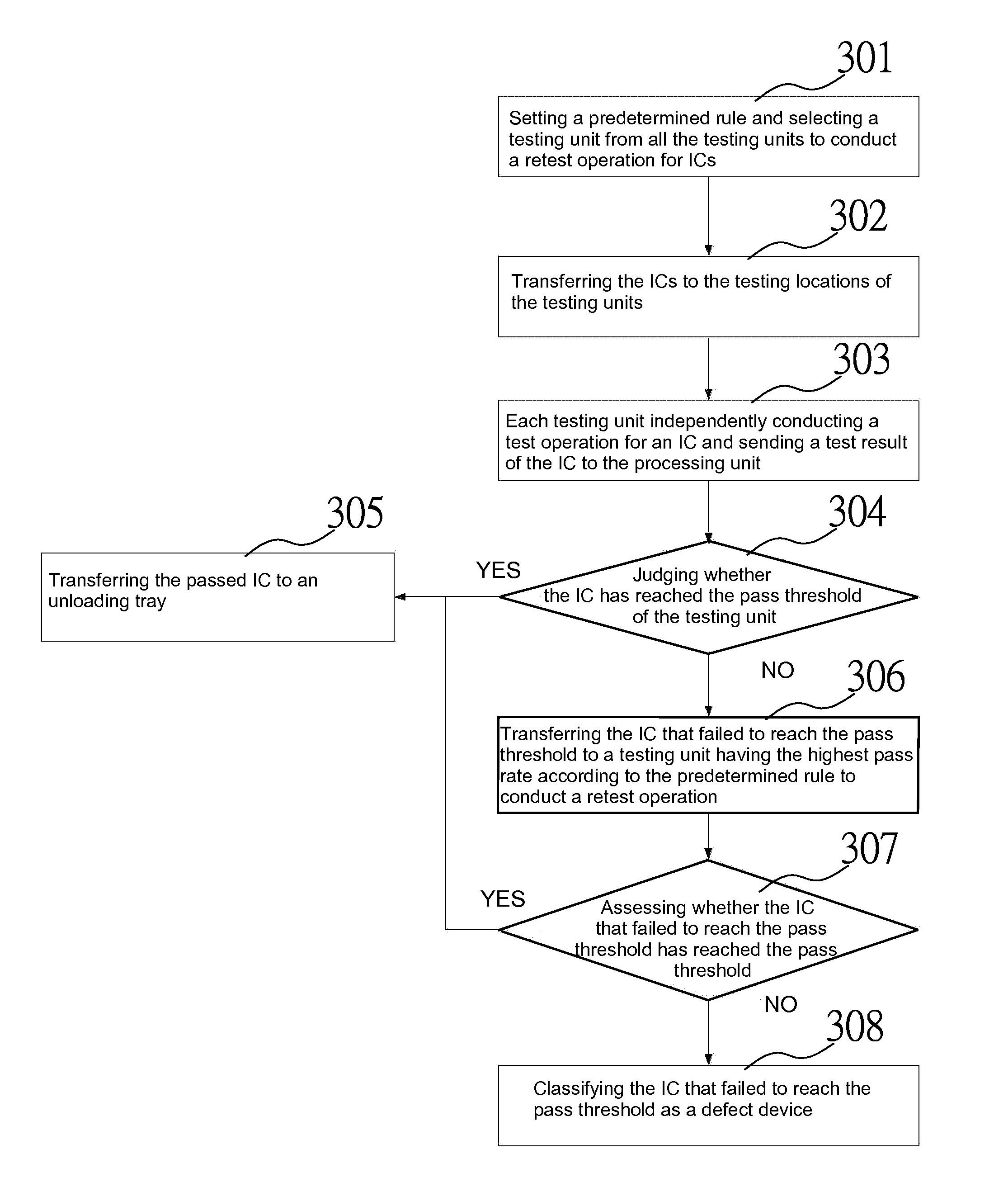
[0031]FIG. 3 shows a flowchart according to the present invention to proceed with an IC test. First, at the step 301, a predetermined rule is set and stored in the memory device 130, wherein the predetermined rule is set to select a testing unit from the multiple testing units 12 to conduct a retest operation for an IC chip 2 failed to reach the pass threshold of the testing unit, wherein the selected testing unit 12 has a highest pass rate among the multiple testing units 12.

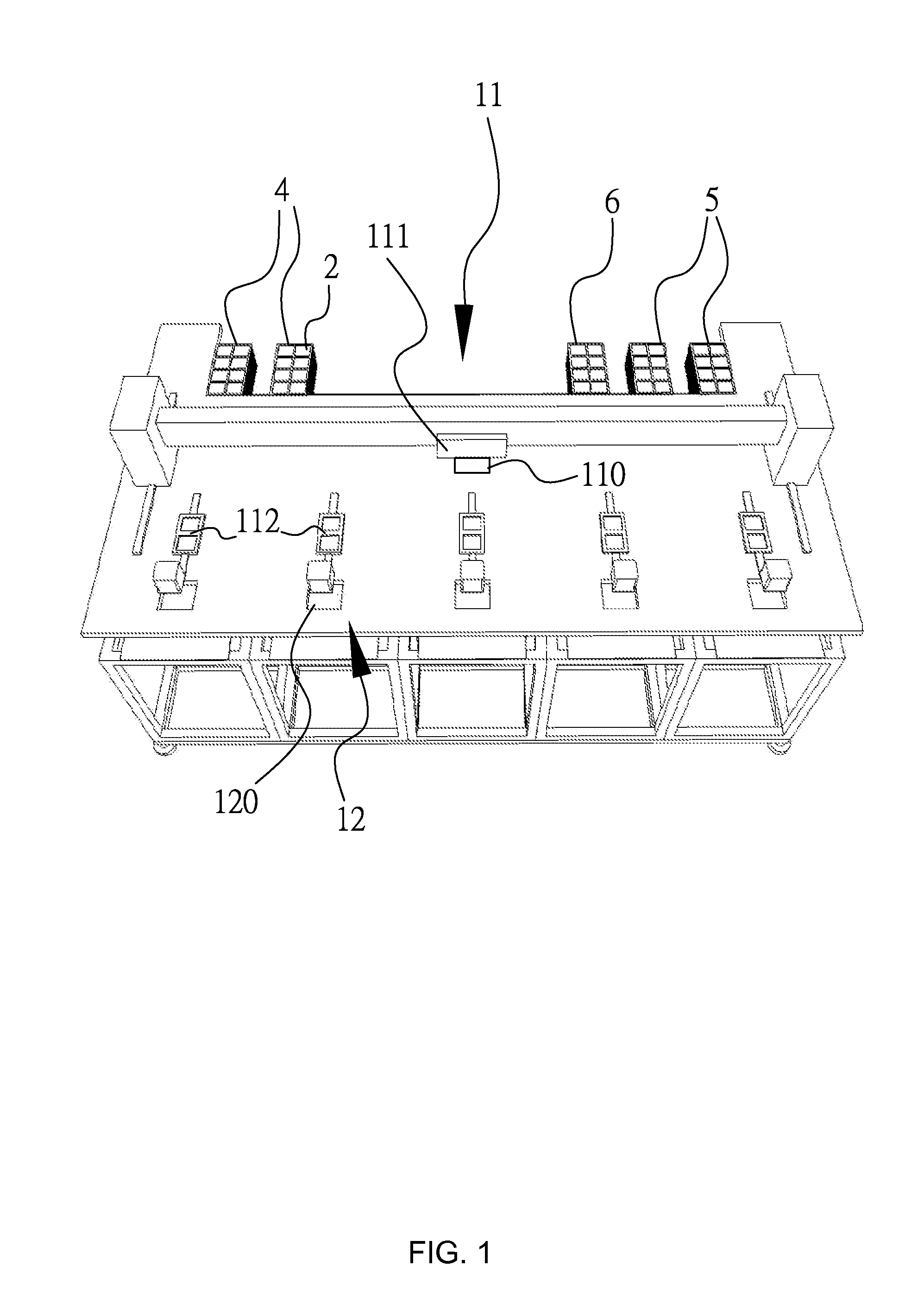
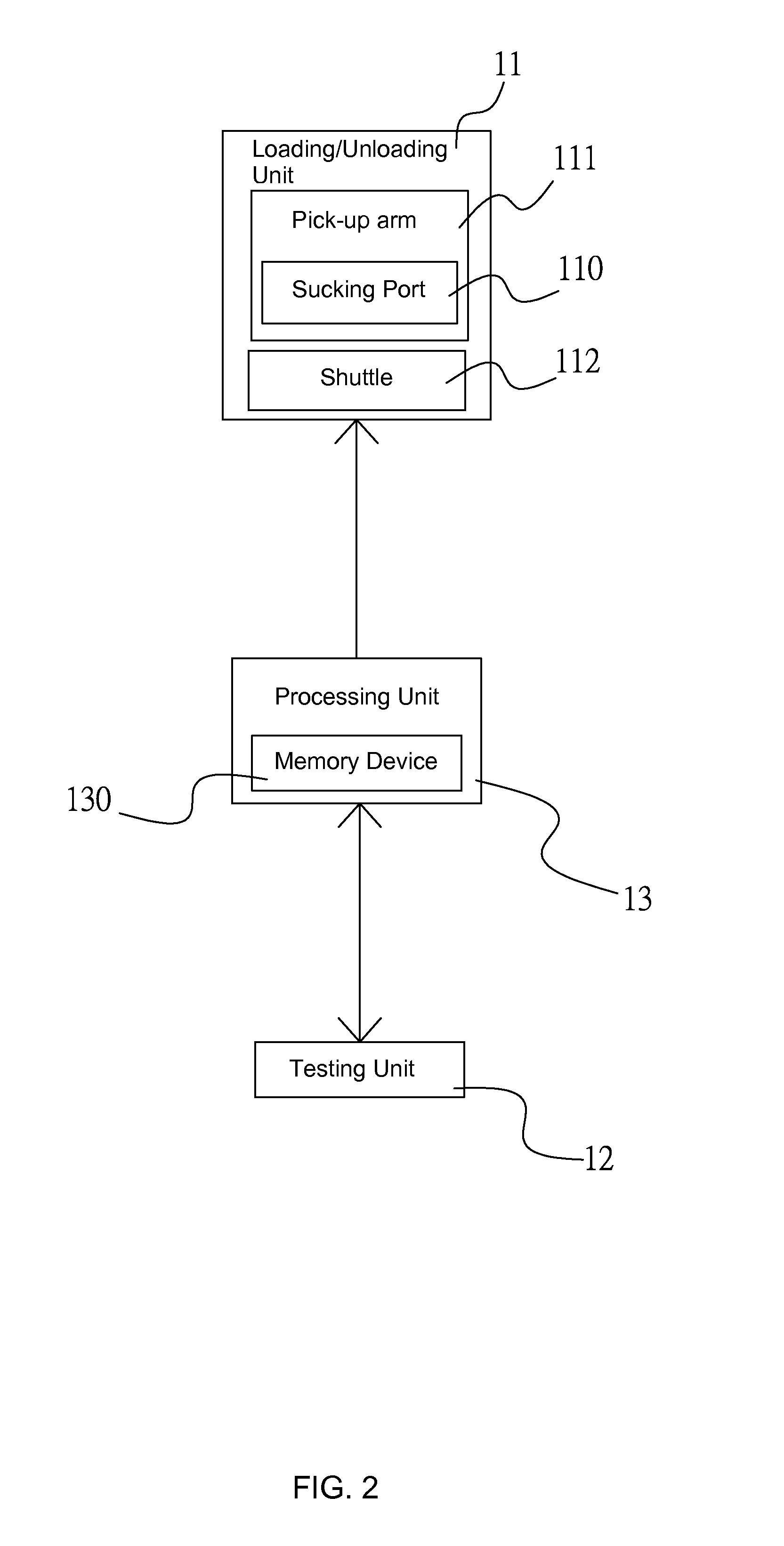
[0032]Next, at the step 302, the pick-up arm 111 of the loading / unloading unit 11 picks up the IC chips 2 from a loading tray 4 using the sucking port 110 and place onto the shuttles 112 corresponding to the respective testing units 12 for transferring the IC chips 2 to the testing locations of the testing units 12. At the step 303, the testing units 12 independently conduct a test operation for the IC chips 2 positioned at the testing locations associated thereto and transmit a test result of the IC chips to t...

second embodiment

[0035]Of course, some IC chips may be required to meet a higher standard, according to which the IC chips will be regarded as qualified devices only when they successfully pass the retest conducted by the original testing units 12. For this reason, the present invention provides a second embodiment, as shown in FIG. 4. In this embodiment, at the step 301′, the predetermined rule stored in the memory device 130 is set to select the testing unit used to inspect an IC chip 2 during the test operation to conduct a retest operation on IC chip 2 when the IC chip 2 failed to reach the pass threshold of the testing unit. If the IC chip still fails in the retest operation, the IC will be regarded as nonconformance with the higher standard. However, the IC can still be classified as a downgrade, or alternatively, another testing unit can be selected to conduct a retest operation again for the IC.

[0036]Accordingly, the step 300′ and the step 310′ can be added following the step 304. According ...

third embodiment

[0037]The test approach used in the present invention is generally the same as the previous embodiments except that the predetermined rule stored in the memory device 130 is changed. Please refer to FIG. 5 taken in conjunction with FIGS. 1 and 2 for a better understanding. At the step 301″, a predetermined rule will be set and stored in the memory device 130, wherein the predetermined rule is set to select one of the testing units that provides a predetermined level of pass rate to conduct a retest operation on an IC chip 2 which has not passed the original test. In this embodiment, for example, the selected testing unit must have an accumulated pass rate of greater than 70% in the past three days. In addition, the predetermined rule can be further limited such that, when the IC chip 2 is to be subjected to retest, the testing unit originally used to conduct the test operation for the IC chip 2 is excluded from being selected for the retest operation. Accordingly, at the step 304, i...


PUM


Abstract

An automatic retest method for a system-level IC test equipment and the IC test equipment is disclosed, wherein the IC test equipment includes multiple testing units, a loading/unloading unit, and a processing unit; each testing unit is capable of testing an IC individually and has a pass rate. When the testing unit finishes a test operation, it will send test report of the IC to the processing unit. The processing unit will determine whether the IC has reached a pass threshold of the testing unit. The processing unit will issue a command, according to a predetermined rule, to transfer the IC that failed to reach the pass threshold to one of the testing units conforming to the predetermined rule to conduct a retest operation. Finally, the processing unit will confirm whether the IC that failed to reach the pass threshold has reached the pass threshold in the retest operation.

Description

FIELD OF THE INVENTION[0001]The present invention relates to a system-level IC test equipment and, more particularly, to an automatic retest method for a system-level IC test equipment and the IC test equipment using the same.BACKGROUND OF THE INVENTION[0002]With the rapid development of semiconductor technology, the IC chips are becoming to have more complicated structures. In fabricating electronic products, a mechanical or automatic way of mounting electronic components onto PCBs (printed circuit boards) has been used extensively to replace the conventional manual way. A full automatic process is involved with IC (integrated circuit) fabrication, IC inspection, IC sorting, mounting and soldering IC chips onto PCBs, and final product inspection. The purpose of employing the automatic process is to effectively eliminate the defect components in a shorter time to ensure the quality of the final product. Therefore, the stability and accuracy of the test machine is a key element in de...

Claims


Application Information

Patent Timeline
Patent Type & Authority Applications(United States)
IPC IPC(8): G01R31/28
CPCG01R31/2894G01R31/287
Inventor OUYANG, CHIN-YIHSU, LIANG-YU
Owner CHROMA ATE
Why Eureka
Try Eureka