Patterning method
a pattern and overlay technology, applied in the direction of semiconductor/solid-state device manufacturing, basic electric elements, electric apparatus, etc., can solve the problems of large challenge to pattern placement and overlay, insufficient resolution of current machines, and the inability to fabricate a smaller cd
- Summary
- Abstract
- Description
- Claims
- Application Information
AI Technical Summary
Benefits of technology
Problems solved by technology
Method used
Image
Examples
first embodiment
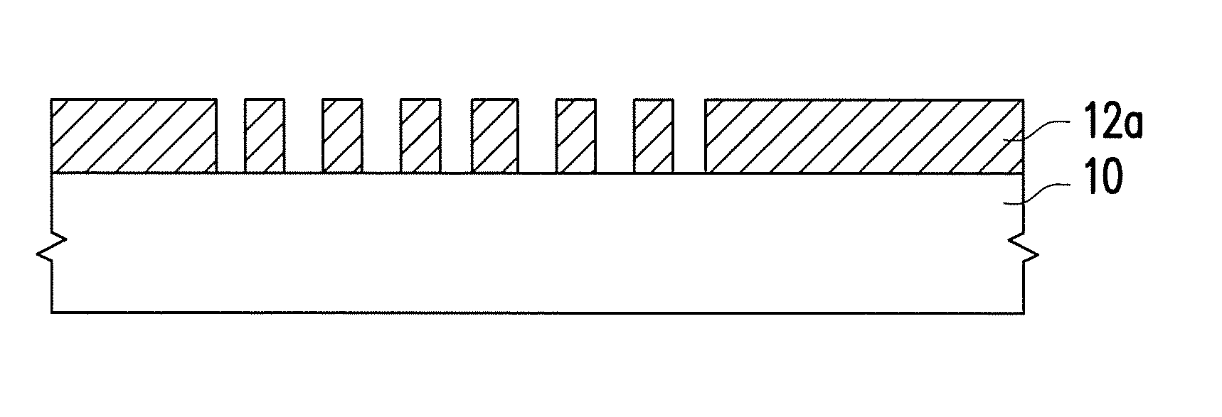
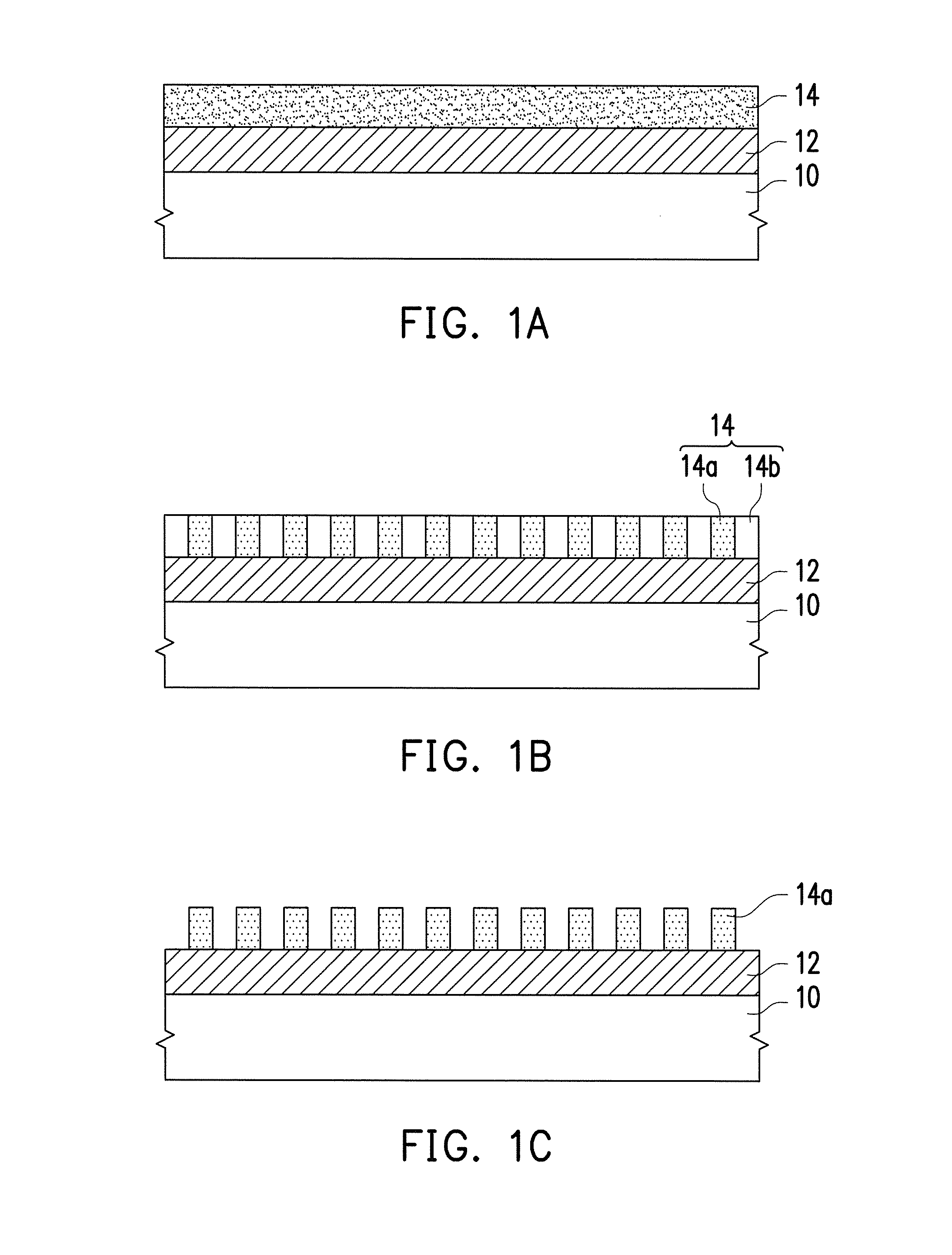
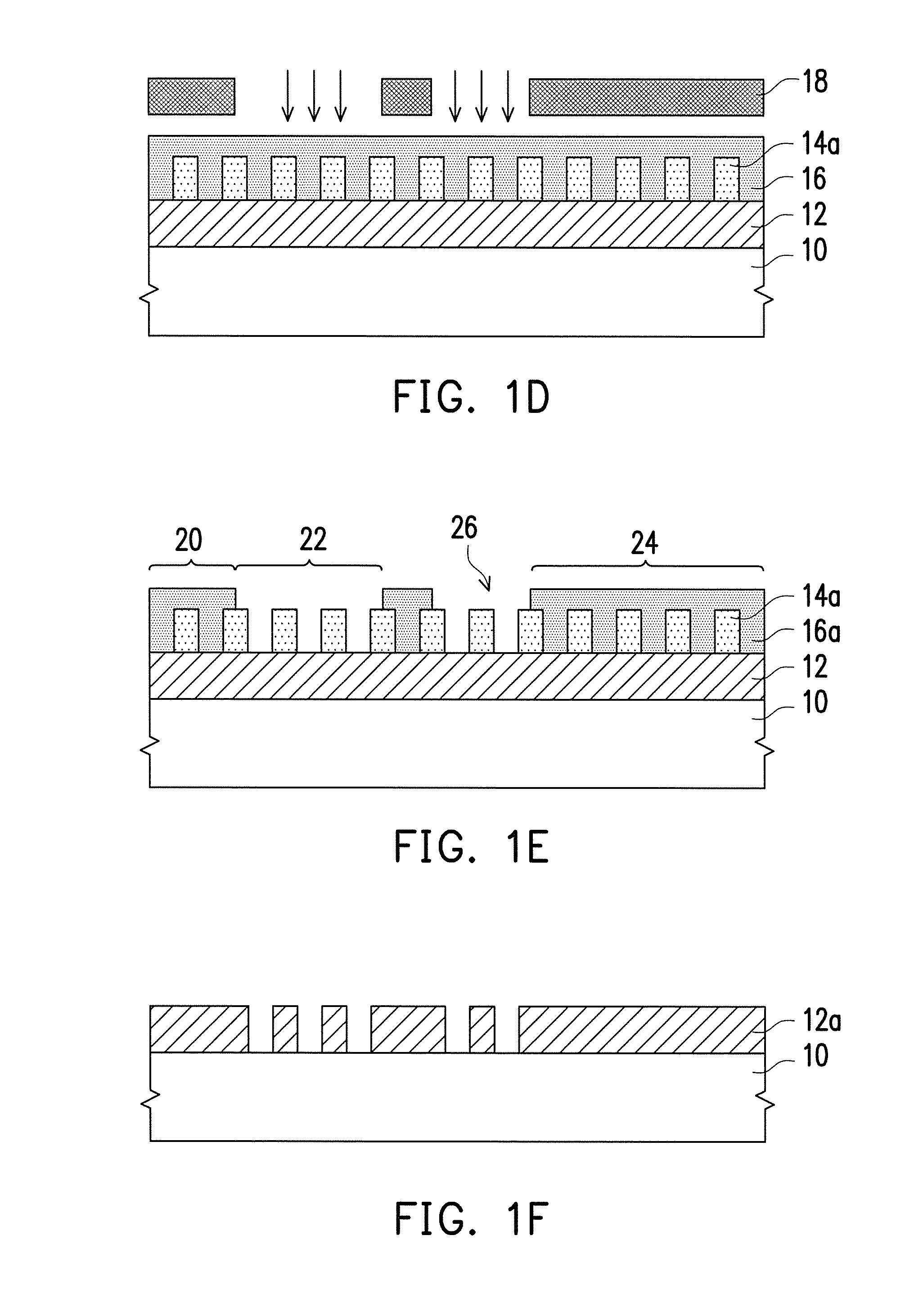
[0029]FIG. 1A to FIG. 1F are cross-sectional diagrams of the process of a patterning method illustrated according to the concept of the invention.
[0030]Referring to FIG. 1A, a substrate 10 is provided. The substrate 10 in the invention can include a semiconductor material, an insulating material, a conductive material, or any combination of the materials, and includes a multi-layer structure. For instance, the substrate 10 can be formed by at least one semiconductor material selected from the group consisting of Si, Ge, SiGe, GaP, GaAs, SiC, SiGeC, InAs, and InP. Moreover, a silicon on insulator (SOI) substrate can also be used. The substrate 10 can be formed by a multi-layer material, such as Si / SiGe or Si / SiC. The substrate 10 can include one layer or more than one layer of a material, such as a dielectric layer, a barrier layer SiC for blocking copper, such as a metal layer of copper, a hafnium oxide layer, a silicon layer, a silicon oxide layer, an analogue thereof, or a combina...
second embodiment
[0037]FIG. 2A to FIG. 2F are cross-sectional diagrams of the process of a patterning method illustrated according to the concept of the invention.
[0038]Referring to FIG. 2A, a material layer 12, a hard mask layer 60, and a DSA material layer 54 are formed on a substrate 10 in sequence. The material, thickness, and forming method of each of the substrate 10 and the material layer 12 are as described for each of the substrate 10 and the material layer 12 of the first embodiment above and are not repeated herein. The material, thickness, and forming method of the DSA material layer 54 can be the same as the material, thickness, and forming method of the DSA material 14 and are not repeated herein. The hard mask layer 60 can include any suitable semiconductor material, insulating material, or conductive material such as silicon oxide, silicon nitride, silicon oxynitride, a metal, metal nitride, a polysilicon material, or a combination thereof, but is not limited thereto. The forming met...
PUM
 Abstract
Description
Claims
Application Information


