

Semiconductor photoelectrode and method for splitting water photoelectrochemically using photoelectrochemical cell comprising the same
a technology of photoelectrode and semiconductors, which is applied in the direction of electrode coating, physical/chemical process catalysts, instruments, etc., can solve the problems of inexhaustible hydrogen formation in water splitting and difficulty in moving secondary batteries, and achieve the effect of improving the generation efficiency of hydrogen and high quantum efficiency
- Summary
- Abstract
- Description
- Claims
- Application Information
AI Technical Summary
Benefits of technology
Problems solved by technology
Method used
Image

Examples
first embodiment
[0052]FIG. 6 shows a semiconductor photoelectrode 200 according to the first embodiment. The semiconductor photoelectrode 200 comprises a first semiconductor photocatalyst layer 202 disposed on the surface of a conductive substrate 102 and a second semiconductor photocatalyst layer 203 disposed on the surface of the first semiconductor photocatalyst layer 202. The first semiconductor photocatalyst layer 202 has a surface shape similar to pillar protrusions formed on the surface of the conductive substrate 102. The second semiconductor photocatalyst layer 203 also has a surface shape similar to pillar protrusions formed on the surface of the first semiconductor photocatalyst layer 202. The first semiconductor photocatalyst layer 202 is sandwiched between the conductive substrate 102 and the second semiconductor photocatalyst layer 203. The front surface of the first semiconductor catalyst layer 202 is in contact with the back surface of the second semiconductor photocatalyst layer 20...
second embodiment
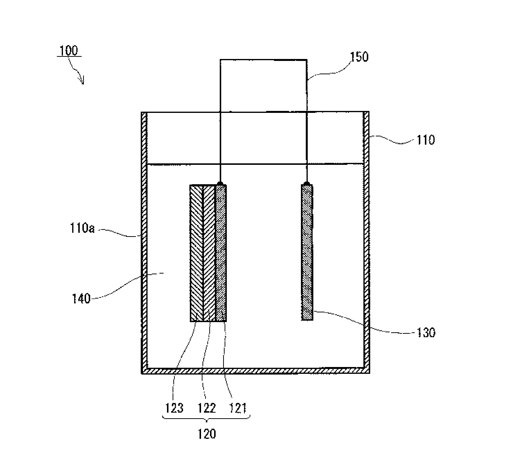
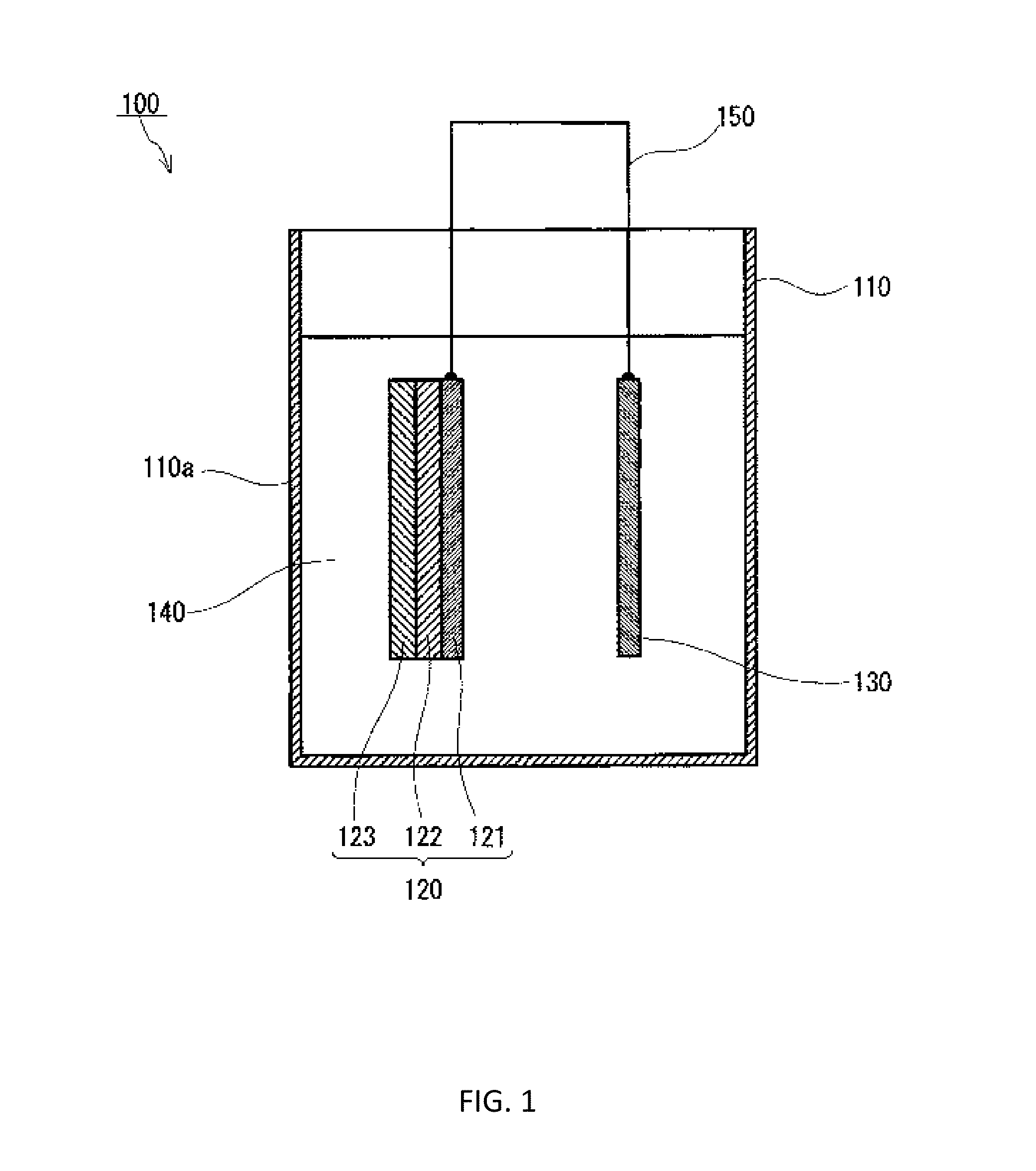
[0114]FIG. 9 shows a photoelectrochemical cell according to the second embodiment of the present invention. As shown in FIG. 9, the photoelectrochemical cell 300 according to the second embodiment comprises a container 31, a semiconductor photoelectrode 200, a counter electrode 32, and a separator 35. The semiconductor photoelectrode 200, the counter electrode 32, and the separator 35 are contained in the container 31. The inside of the container 31 is divided into a first chamber 36 and a second chamber 37 by the separator 35. The semiconductor photoelectrode 200 is disposed in the first chamber 36, whereas the counter electrode 32 is disposed in the second chamber 37. A liquid such as an aqueous electrolyte solution 33 is stored in both the first chamber 36 and the second chamber 37. The separator 35 is not need to be provided.
[0115]The semiconductor photoelectrode 200 is disposed in the first chamber 36 so as to be in contact with the aqueous electrolyte solution 33. The semicond...
referential examples
Referential Example 1
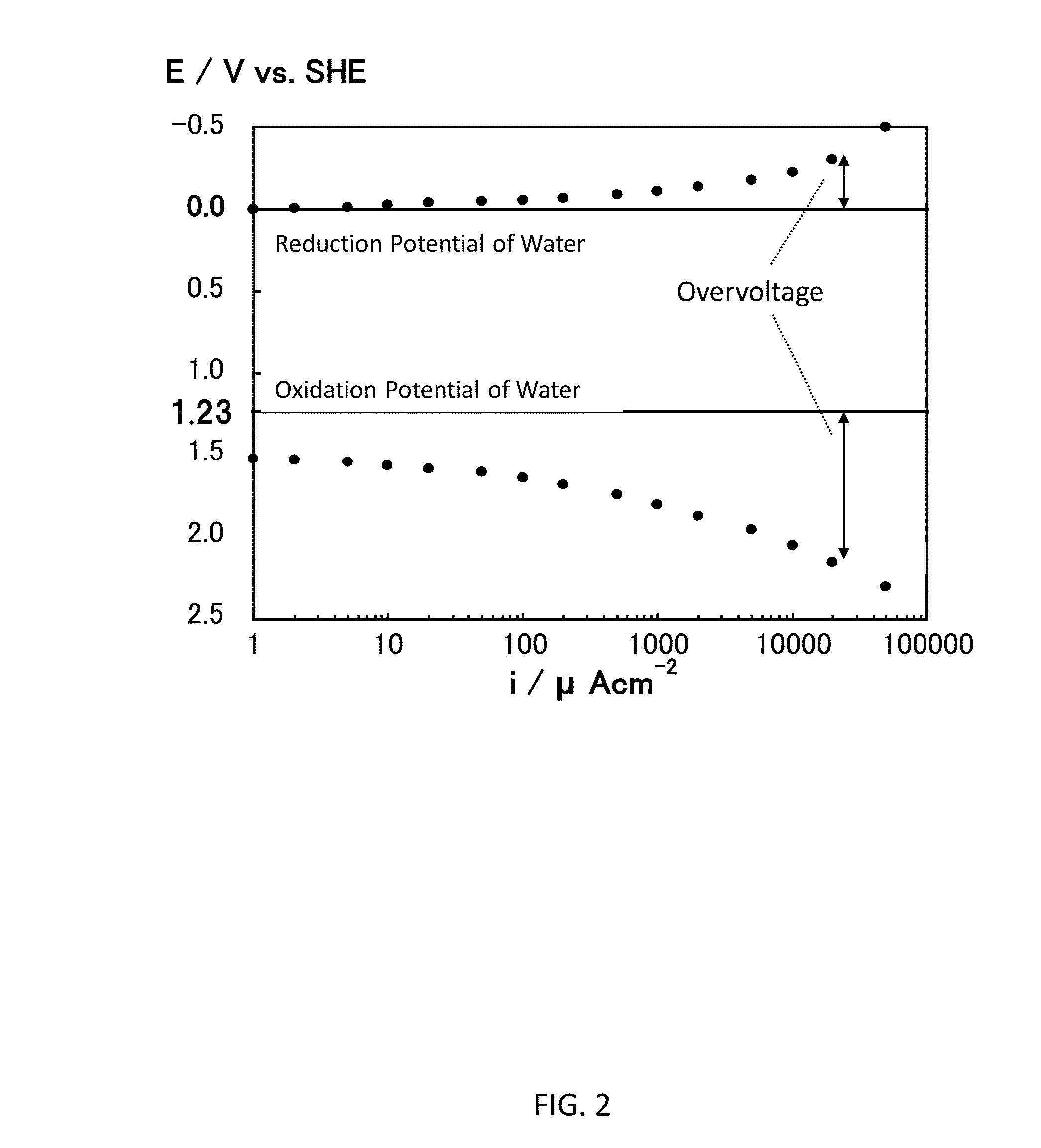
[0129]In order to discuss a desirable thickness of the first semiconductor layer 202, a semiconductor photocatalyst layer formed of a TiO2 film was used. The present inventors discussed the relationship between the thickness of the TiO2 film and the quantum efficiency as below.
[0130]First, a TiO2 film having a thickness of 22 nanometers was formed on a transparent electrode substrate made of indium tin oxide (hereinafter, referred to as “ITO”) by a sputtering method to provide a sample A1. Similarly, provided were samples A2, A3, and A4 having a TiO2 film having a thickness of 110 nanometers, 220 nanometers, and 660 nanometers, respectively. Since the samples A1-A4 were used for discussion of the relationship between the semiconductor photocatalyst layer and the quantum efficiency, the transparent electrode substrate did not have pillar protrusions on the surface thereof. In other words, the surface of the transparent electrode substrate was flat-and-smooth.
[013...
PUM
| Property | Measurement | Unit |
|---|---|---|
| thickness | aaaaa | aaaaa |
| thickness | aaaaa | aaaaa |
| distance | aaaaa | aaaaa |
Abstract
Description
Claims
Application Information