

Organic light emitting display device
- Summary
- Abstract
- Description
- Claims
- Application Information
AI Technical Summary
Benefits of technology
Problems solved by technology
Method used
Image

Examples
first embodiment
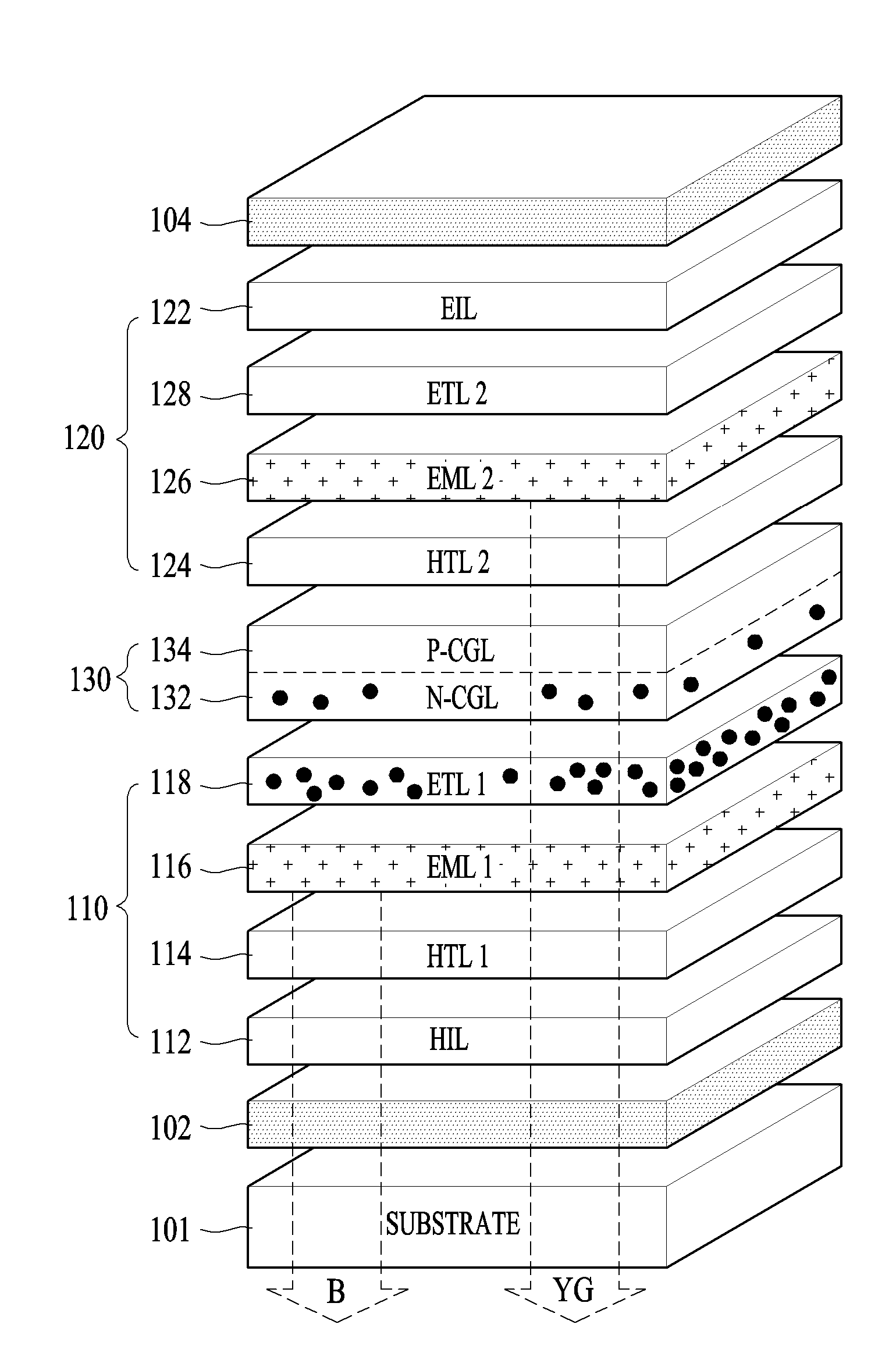
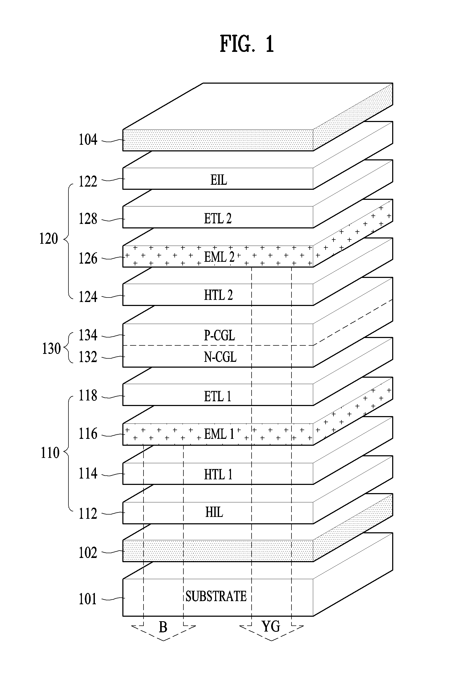
[0039]FIG. 1 is a perspective view illustrating an organic light emitting display (OLED) device according to the present invention.
[0040]Referring to FIG. 1, the OLED device includes first and second electrodes 102 and 104 facing each other on a substrate 101, first and second light emitting units 110 and 120 formed between the first and second electrodes 102 and 104, and a charge generation layer 130 provided between the first and second light emitting units 110 and 120.
[0041]At least one of the first and second electrodes 102 and 104 is formed of a semi-transparent electrode. In a case in which the first electrode 102 is a semi-transparent electrode and the second electrode 104 is a reflective electrode, the OLED device is a rear light emitting structure in which light is emitted downward. In a case in which the second electrode 104 is a semi-transparent electrode and the first electrode 102 is a reflective electrode, the OLED device is a front light emitting structure in which li...
second embodiment
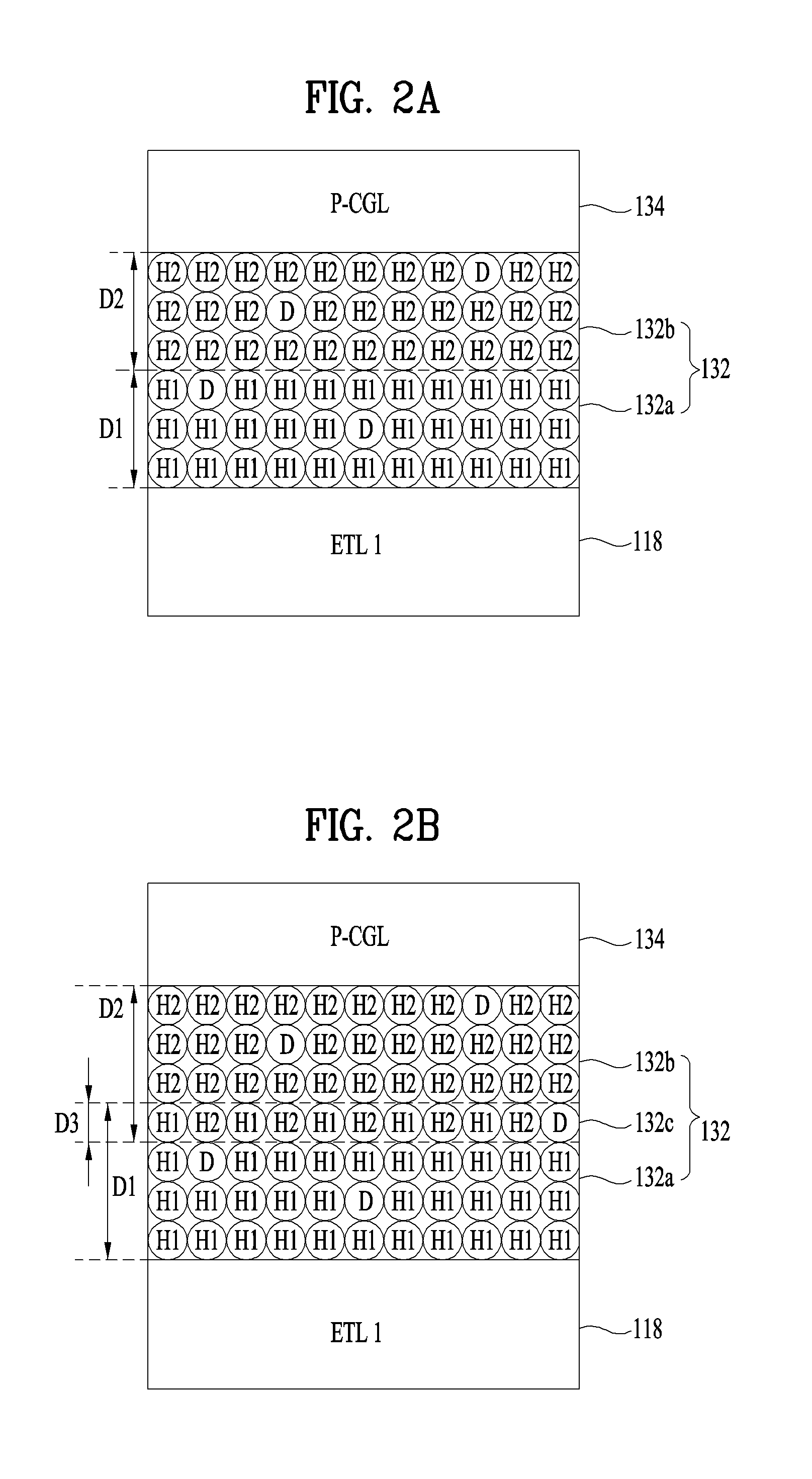
[0066]FIG. 7 is a perspective view illustrating an OLED device according to the present invention. The OLED device illustrated in FIG. 7 is substantially identical to what is shown in FIG. 1, except that an N-type charge generation layer and a first electron transport layer include the same host. Thus, a detailed description of the identical elements will be omitted.
[0067]Referring to FIG. 7, a first electron transport layer 118 is formed of the same material as any one of a plurality of hosts included in an N-type charge generation layer 132. As a result, an energy barrier between the first electron transport layer 118 and the N-type charge generation layer 132 may be reduced or minimized, and thus electrons may be easily injected into the first electron transport layer 118. The first electron transport layer 118 may have a thickness De in a range of about 100 Å to about 500 Å.
[0068]The N-type charge generation layer 132 includes at least two hosts formed of different materials and...
PUM
 Abstract
Description
Claims
Application Information