Semiconductor device

a technology of semiconductor devices and semiconductors, applied in the direction of semiconductor devices, electrical devices, transistors, etc., can solve the problems of failure to apply termination regions, and achieve the effect of improving the breakdown voltage performance of semiconductor devices

Active Publication Date: 2015-04-16
MITSUBISHI ELECTRIC CORP
View PDF12 Cites 5 Cited by
  • Summary
  • Abstract
  • Description
  • Claims
  • Application Information

AI Technical Summary

Benefits of technology

[0010]An object of the present invention is to provide a semiconductor device capable of improving breakdown voltage performance without enlarging an area of the termination region.
[0012]The semiconductor device according to the present invention includes, in the termination region: the breakdown voltage holding region formed in the predetermined depth direction from the surface of the first conductivity-type substrate, the breakdown voltage holding region being the second conductivity-type low-concentration impurity region; the first insulating film on the substrate, the first insulating film formed so as to cover at least the breakdown voltage holding region; the first field plate formed on the first insulating film; the second insulating film formed so as to cover the first field plate and the first insulating film; and the second field plate formed on the second insulating film. The first insulating film is thicker in the corner portion than in the straight portion. Therefore, the breakdown voltage performance of the semiconductor device may be improved without enlarging the area of the termination region.

Problems solved by technology

However, for example, when an identification mark indicating information about the semiconductor device or a control pattern for controlling a semiconductor process condition are already disposed outside the corner portion, there arises a problem of failure to apply the termination region with the wider breakdown voltage holding region formed in the corner portion.

Method used


Image

  • Semiconductor device
  • Semiconductor device
  • Semiconductor device

Examples


first preferred embodiment

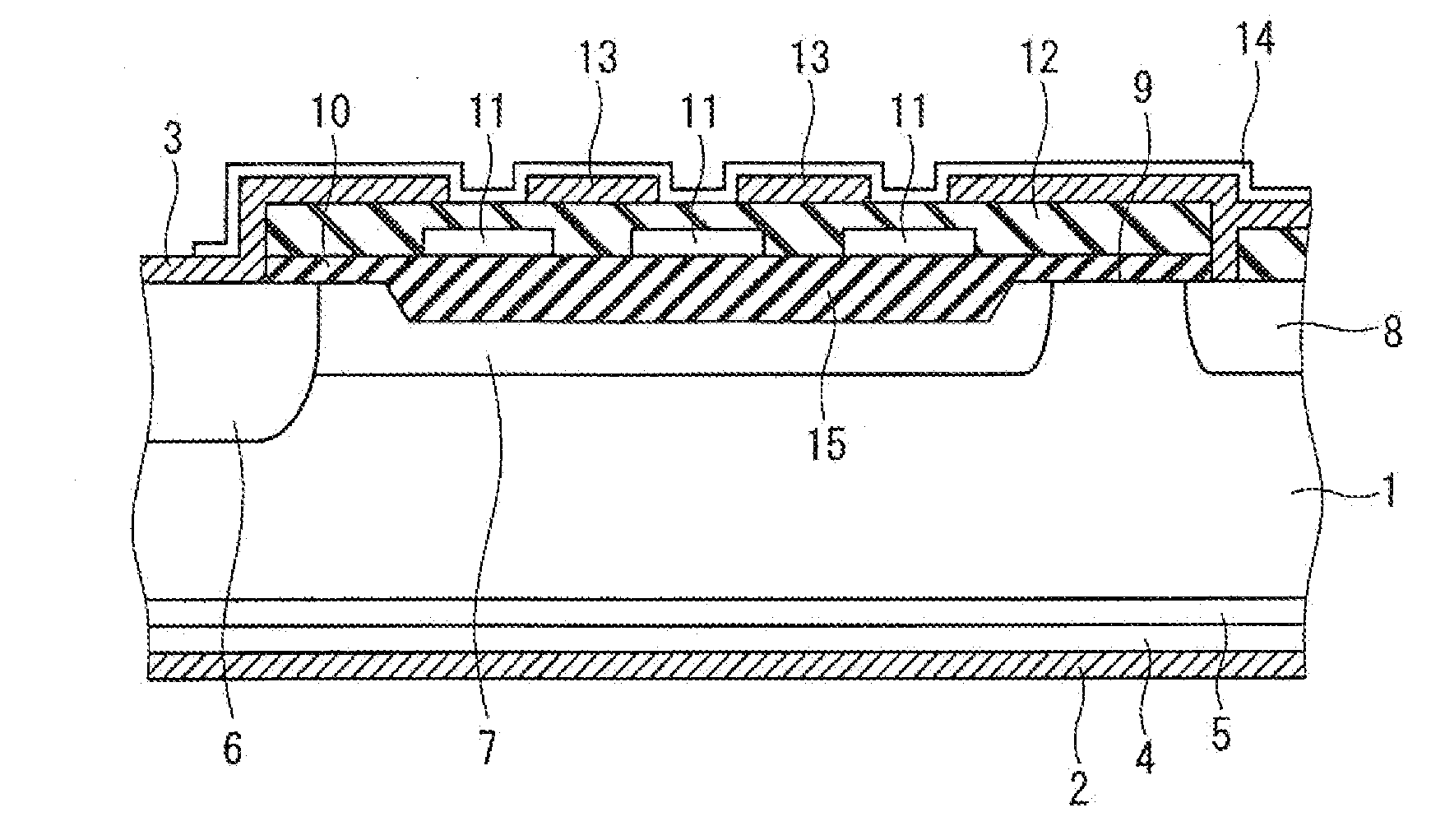
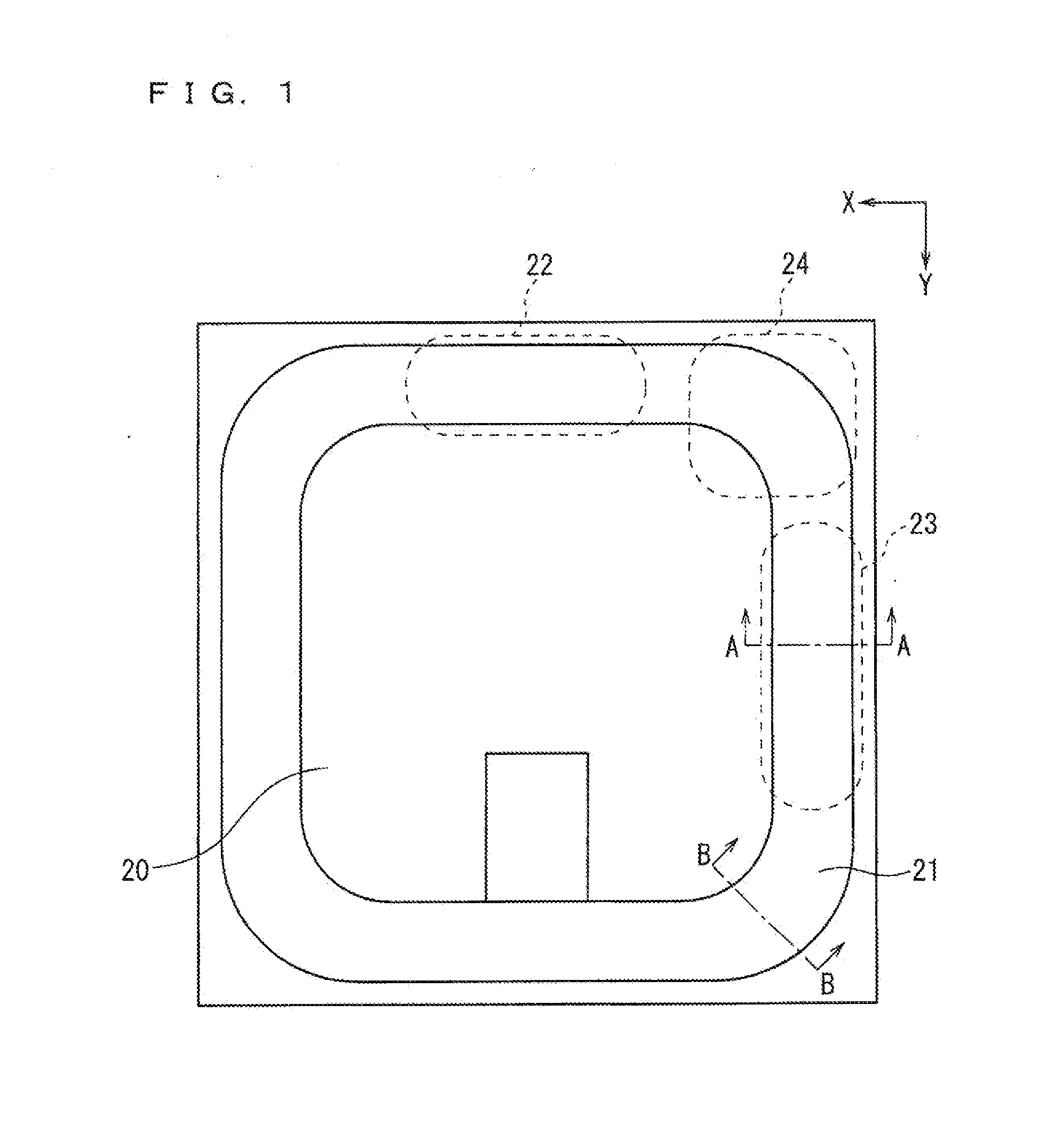
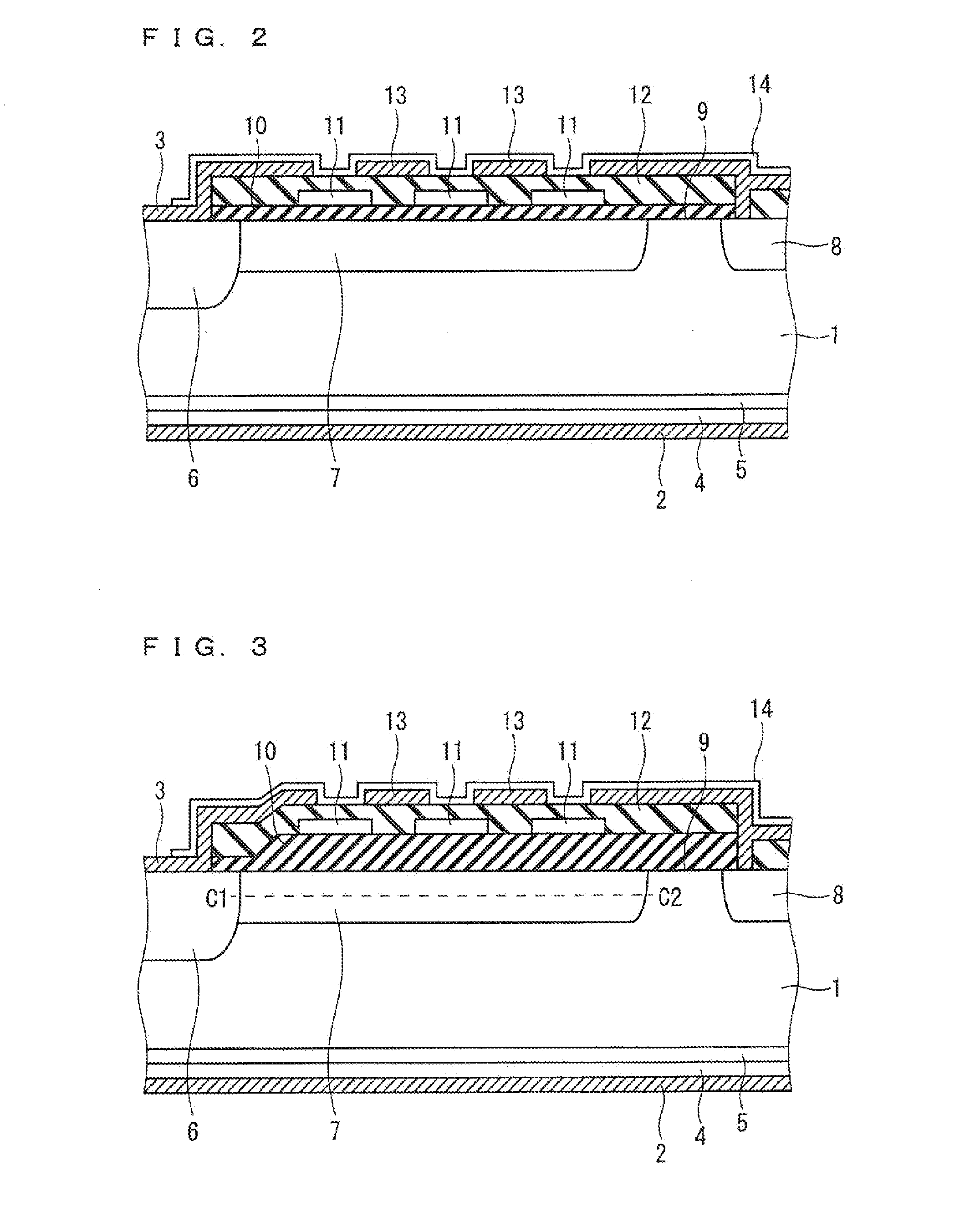
[0048]FIG. 1 is a plan view illustrating an example of a configuration of a semiconductor device according to a first preferred embodiment of the present invention. FIG. 2 is a cross-sectional view illustrating an example of a configuration taken along a line A-A of FIG. 1, and illustrates the configuration of the cross-section of a Y-direction straight portion 23 of a termination region 21. FIG. 3 is a cross-sectional view illustrating an example of a configuration taken along a line B-B of FIG. 1, and illustrates the configuration of the cross-section of a corner portion 24 of the termination region 21. While FIG. 2 illustrates the configuration of the cross-section of the Y-direction straight portion 23, a configuration of a cross-section of an X-direction straight portion 22 is similar thereto.

[0049]As illustrated in FIGS. 1 to 3, in the semiconductor device according to the first preferred embodiment, the first insulating film 10 formed in the termination region 21 is thicker i...

second preferred embodiment

[0060]FIG. 6 is a cross-sectional view illustrating an example of a configuration taken along a line B-B of FIG. 1, and illustrates the configuration of the cross-section of a corner portion 24 of a termination region 21.

[0061]In a second preferred embodiment of the present invention, a substrate surface 9 of an n− type substrate 1 includes a recessed region 15 formed in a recessed shape in the corner portion 24. Other configurations are similar to those in the first preferred embodiment and description will be omitted.

[0062]As illustrated in FIG. 6, the formation of the recessed region 15 in the corner portion 24 enables a first insulating film 10 to be thicker in the corner portion 24 than in an X-direction straight portion 22 and a Y-direction straight portion 23. A surface of the first insulating film 10 may be made flush between the corner portion 24 and a straight portion (the X-direction straight portion 22, the Y-direction straight portion 23).

[0063]Thus, according to the se...

third preferred embodiment

[0064]In a third preferred embodiment of the present invention, a recessed region 15 according to a second preferred embodiment is formed by a local oxidation of silicon (LOCOS) method.

[0065]FIGS. 7 to 9 are diagrams each illustrating an example of a manufacturing process of a semiconductor device according to the third preferred embodiment. In particular, FIGS. 7 to 9 each illustrate an example of a process of forming the recessed region 15.

[0066]As illustrated in FIG. 7, a nitride film 16 is formed on a substrate surface 9 of an n− type substrate 1 so that a portion of a surface of a p− type breakdown voltage holding region 7 is exposed. In other words, the nitride film 16 is formed so that the portion of the substrate surface 9 in which the recessed region 15 is to be formed is exposed.

[0067]Next, as illustrated in FIG. 8, an oxide film 17 having a LOCOS shape is formed by a thermal oxidation process.

[0068]Next, as illustrated in FIG. 9, the recessed region 15 is formed by elimin...


PUM


Abstract

A semiconductor device according to the present invention includes, in a termination region, a p− type breakdown voltage holding region that is an impurity region formed in a predetermined depth direction from a substrate surface of an n− type substrate, a first insulating film formed on the n− type substrate so as to cover at least the p− type breakdown voltage holding region, a first field plate formed on the first insulating film, a second insulating film formed so as to cover the first field plate and the first insulating film, and a second field plate formed on the second insulating film. The first insulating film is thicker in a corner portion than in an X-direction straight portion and a Y-direction straight portion.

Description

BACKGROUND OF THE INVENTION[0001]1. Field of the Invention[0002]The present invention relates to a semiconductor device having a termination region for electric power conversion.[0003]2. Description of the Background Art[0004]Power devices, which are semiconductor devices for electric power conversion, are widely used in various fields from home electric appliances, electric vehicles, railroads, to attention-getting renewable energy, such as photovoltaic power generation and wind power generation. In such fields, power devices or power electronics apparatuses equipped with the power devices are used for conversion of electric power energy. Higher performance, such as reduction in size and higher efficiency, has been desired.[0005]A power device includes an element region provided in a center of a chip and a termination region provided in a peripheral portion of the element region. The element region primarily passes electric current. The termination region has a breakdown voltage. A...

Claims


Application Information

Patent Timeline
Patent Type & Authority Applications(United States)
IPC IPC(8): H01L29/40H01L29/06
CPCH01L29/402H01L29/063H01L29/0661H01L29/404H01L29/66333H01L29/66712H01L29/7395H01L29/7811H01L29/0638H01L29/0696H01L29/8611
Inventor KAMIBABA, RYUTAGUCHI, KENSUKE
Owner MITSUBISHI ELECTRIC CORP
Why Eureka
Try Eureka