Episubstrates for Selective Area Growth of Group III-V Material and a Method for Fabricating a Group III-V Material on a Silicon Substrate

a silicon substrate and selective area technology, applied in the field of silicon substrates, can solve the problems of forming cracks in the nitride layer, crystal defects, tensile stress,

Inactive Publication Date: 2015-04-30
INTERUNIVERSITAIR MICRO ELECTRONICS CENT (IMEC VZW)
View PDF2 Cites 4 Cited by
  • Summary
  • Abstract
  • Description
  • Claims
  • Application Information

AI Technical Summary

Problems solved by technology

However, a growth of continuous nitride layers on a silicon substrate leads to the generation of crystal defects due to the difference between the lattice constant and thermal expansion coefficients of the silicon substrate and the nitride layers respectively.
The difference in the thermal expansion coefficient of the silicon substrate and nitride layers results in the generation of a tensile stress during the formation of the nitride layer, which i...

Method used


Image

  • Episubstrates for Selective Area Growth of Group III-V Material and a Method for Fabricating a Group III-V Material on a Silicon Substrate
  • Episubstrates for Selective Area Growth of Group III-V Material and a Method for Fabricating a Group III-V Material on a Silicon Substrate
  • Episubstrates for Selective Area Growth of Group III-V Material and a Method for Fabricating a Group III-V Material on a Silicon Substrate

Examples


Embodiment Construction

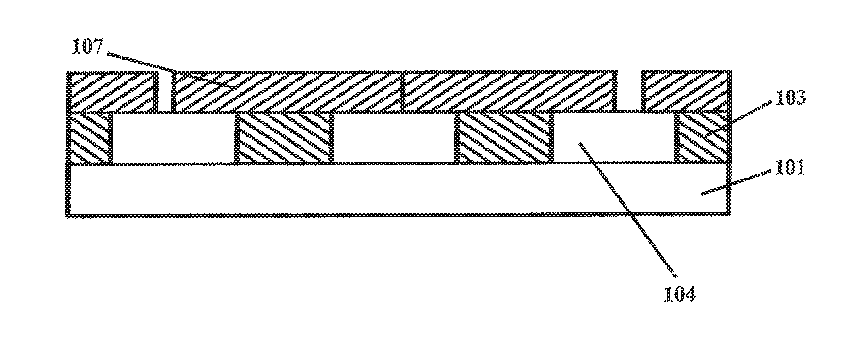
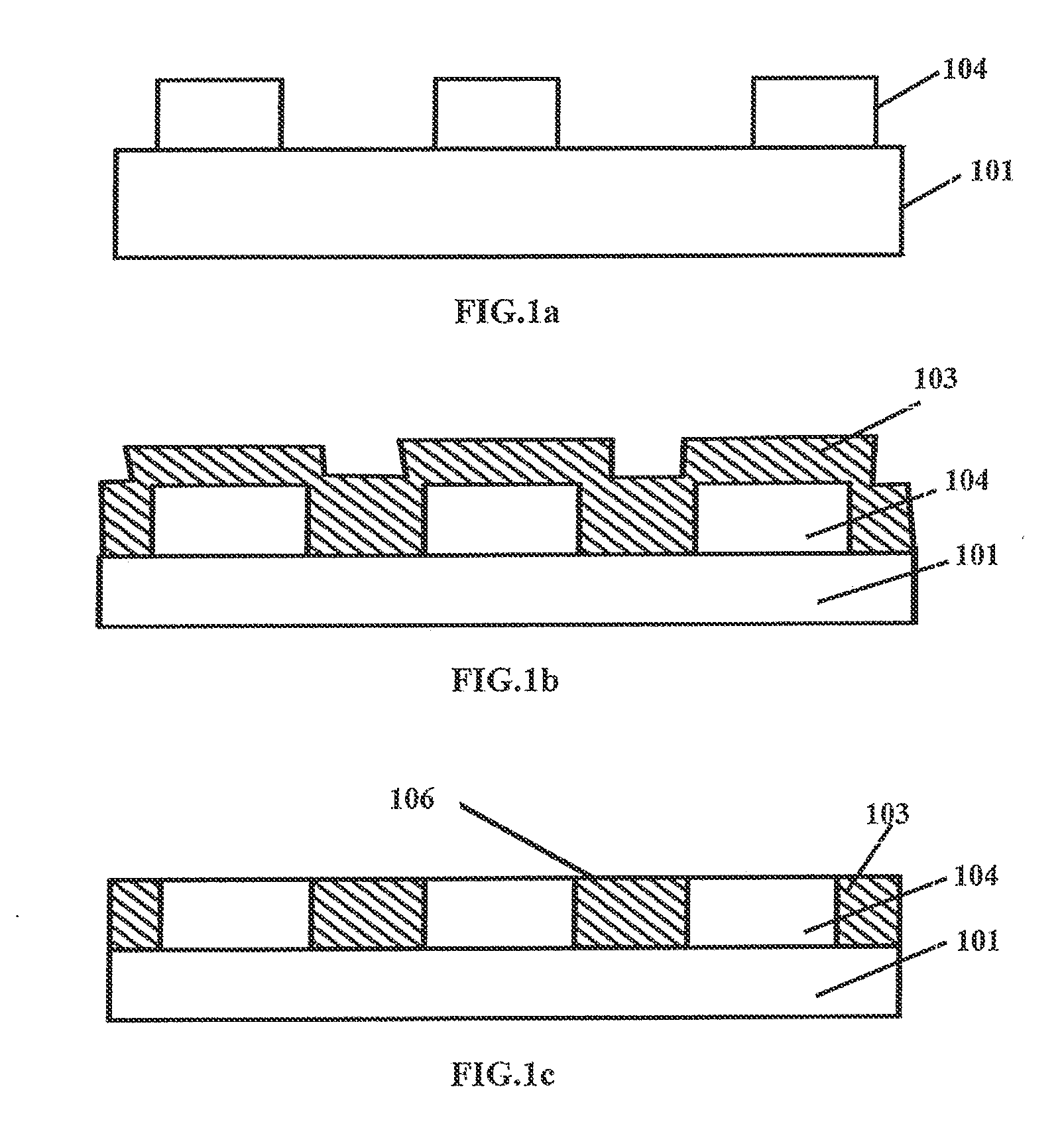
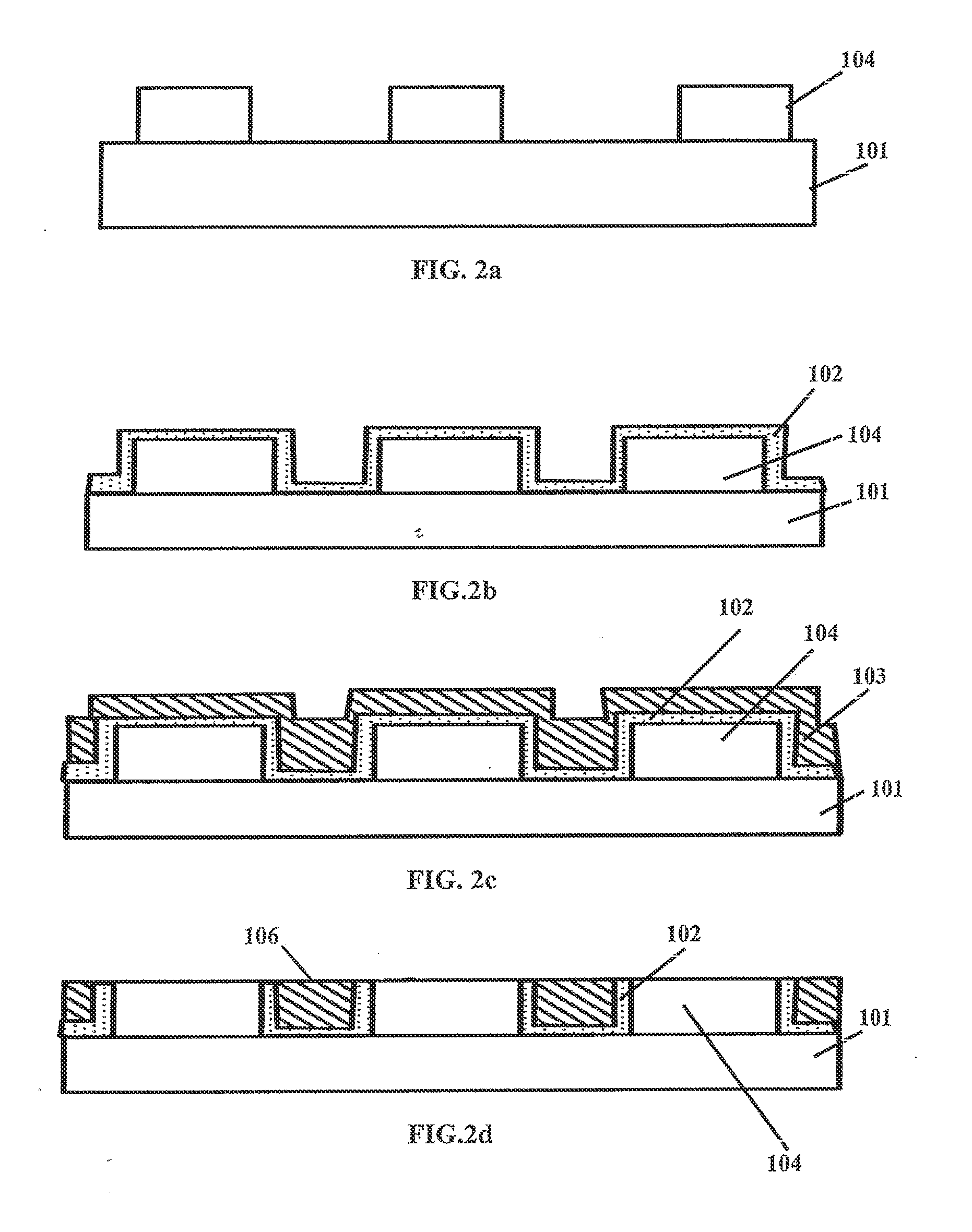
[0008]The primary object of the embodiments of the present disclosure is to provide a method for fabricating silicon substrates with a selective area growth of Group III-V material layer and free of crystal defects.

[0009]Another object of the embodiments of the present disclosure is to provide a method of fabricating silicon substrates with a selective area growth of Group III-V material layer to significantly reduce a formation of cracks in the Group III-V material layers such as group III-V nitride layers.

[0010]Yet another object of the embodiments of the present disclosure is to provide a method of fabricating silicon substrates with a selective area growth of Group III-V material layer to provide an effective stress management during the process of fabrication of a group III-V nitride layer on the silicon substrate.

[0011]Yet another object of the embodiments of the present disclosure is to provide a method of fabricating silicon substrates with a selective area growth of Group I...


PUM


Abstract

The embodiments disclose a silicon substrate with a group III-V material and a method for fabricating a group III-V material on a silicon substrate. The method involves providing a silicon substrate. A first layer formed atop the silicon substrate, is subsequently patterned to expose the underlying silicon substrate. A group III-V material layer is formed over the patterned first layer and also on the exposed silicon substrate. The group III-V material layer is subjected to chemical mechanical polishing (CMP) to expose the first layer resulting in the formation of a plurality of areas suitable for growing a device layer on the silicon substrate.

Description

CROSS-REFERENCE[0001]The present disclosure application claims priority from European patent application no. EP 13190704.0, filed on Oct. 29, 2013, which is incorporated by reference in its entirety.TECHNICAL FIELD[0002]The present disclosure generally relates the silicon substrates and particularly relates the silicon substrates for growing a group III-V material on selective areas. The present disclosure more particularly relates to episubstrates with the selective area growth of group III-V material for use in lighting and power electronics applications.BACKGROUND OF THE DISCLOSURE[0003]Silicon substrates are well known for their properties such as low cost, large wafer size, relatively higher thermal conductivity and higher electrical conductivity. The ability of the silicon substrates to be integrated with diversified electronic circuits renders them suitable for utilization in domains such as lighting and power electronics applications. Further, the aforementioned advantageous...

Claims


Application Information

Patent Timeline
IPC IPC(8): H01L29/20H01L33/12H01L21/306H01L29/201H01L21/02H01L33/00H01L33/32
CPCH01L29/2003H01L33/0066H01L33/0075H01L33/0025H01L33/12H01L21/30625H01L29/201H01L21/02381H01L21/0254H01L21/02488H01L21/02164H01L33/32H01L21/02458H01L21/02639H01L21/02647B24B37/042H01L21/02002
Inventor MOTSNYI, VASYLDUTTA, BARUNDEBROSMEULEN, MAARTEN
Owner INTERUNIVERSITAIR MICRO ELECTRONICS CENT (IMEC VZW)
Why Eureka
Try Eureka