Semiconductor device packages and methods of manufacturing the same

a technology of semiconductor devices and packaging, applied in the direction of manufacturing tools, non-electric welding apparatus, welding apparatus, etc., can solve the problems of increased deterioration of thermomechanical reliability and/or long-time reliability, and increase of failure rate and/or reliability. , to achieve the effect of high reliability and high performan

Active Publication Date: 2015-04-30
SAMSUNG ELECTRONICS CO LTD
View PDF5 Cites 43 Cited by
  • Summary
  • Abstract
  • Description
  • Claims
  • Application Information

AI Technical Summary

Benefits of technology

[0008]Some example embodiments provide semiconductor device packages having high performance and / or high reliability.
[0010]Some example embodiments provide semiconductor device packages having excellent long-time reliability and / or excellent thermo-mechanical reliability.

Problems solved by technology

In the case that the re-melting temperature of a bonding layer between the power device and the substrate is relatively low, thermo-mechanical reliability and / or long-time reliability may be deteriorated and restrictions on use temperature may occur.
In the case where a relatively high pressure process is used in forming the bonding layer, the power device (e.g., semiconductor chip) and the substrate may be damaged due to an applied pressure, thereby causing increase of failure rate and / or deterioration of reliability.
In the event that the bonding layer includes pores or cavities, these may act as a crack initiation site or a crack propagation path, thereby causing deterioration of long-time reliability.
Further, in the case that the thermal conductivity of the bonding layer is relatively low, it may be difficult to secure desired heat dissipation characteristics.

Method used


Image

  • Semiconductor device packages and methods of manufacturing the same
  • Semiconductor device packages and methods of manufacturing the same
  • Semiconductor device packages and methods of manufacturing the same

Examples


Embodiment Construction

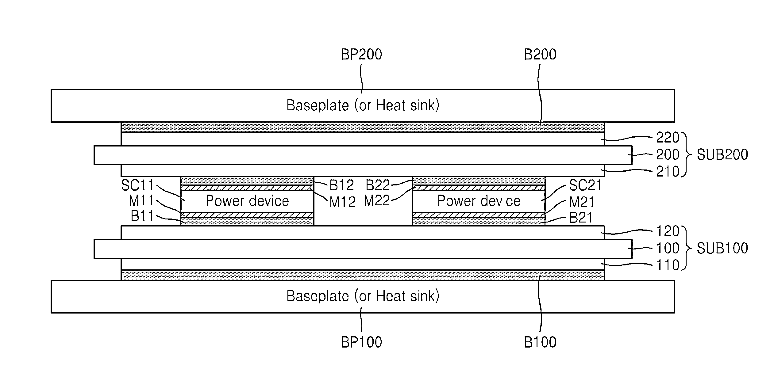
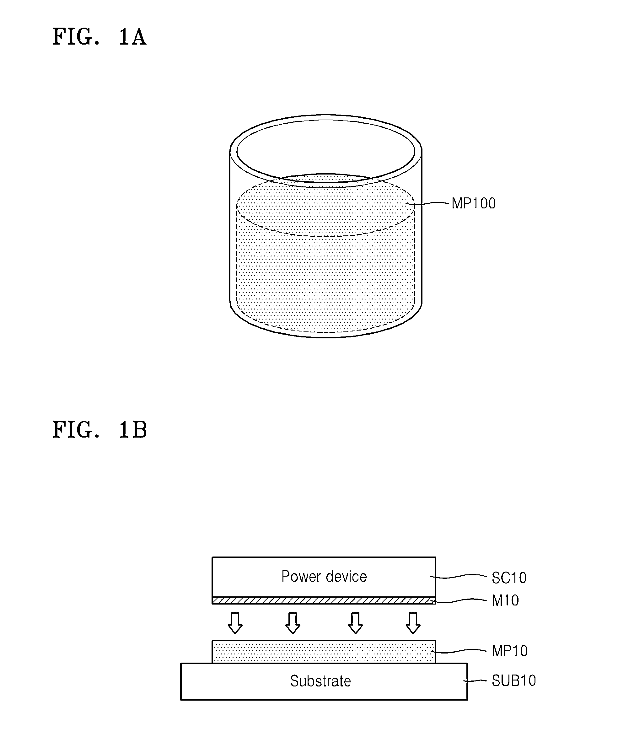
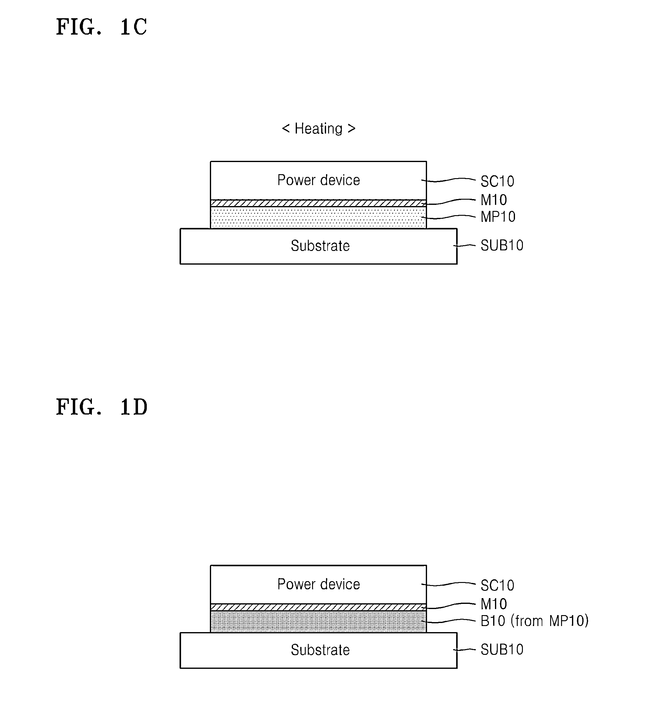
[0069]Various example embodiments will now be described more fully with reference to the accompanying drawings in which some example embodiments are shown.

[0070]It will be understood that when an element is referred to as being“connected” or “coupled” to another element, it can be directly connected or coupled to the other element or intervening elements may be present. In contrast, when an element is referred to as being “directly connected” or “directly coupled” to another element, there are no intervening elements present. As used herein the term “and / or” includes any and all combinations of one or more of the associated listed items.

[0071]It will be understood that, although the terms “first”, “second”, etc. may be used herein to describe various elements, components, regions, layers and / or sections, these elements, components, regions, layers and / or sections should not be limited by these terms. These terms are only used to distinguish one element, component, region, layer or s...


PUM

PropertyMeasurementUnit
pressureaaaaaaaaaa
temperatureaaaaaaaaaa
particle diameteraaaaaaaaaa

Abstract

Semiconductor device packages and methods of manufacturing the semiconductor device packages are provided. A semiconductor device package may include a bonding layer between a substrate and a semiconductor chip, and the bonding layer may include an intermetallic compound. The intermetallic compound may be a compound of metal and solder material. The intermetallic compound may include Ag3Sn. A method of manufacturing the semiconductor device package may include forming a bonding layer, which bonds a semiconductor chip to a substrate, by using a mixed paste including metal particles and a solder material. The bonding layer may be formed by forming an intermetallic compound, which is formed by heating the mixed paste to react the metal particles with the solder material.

Description

RELATED APPLICATIONS[0001]This application claims priority under 35 U.S.C. §119 to Korean Patent Application No. 10-2013-0129570, filed on Oct. 29, 2013 in the Korean Intellectual Property Office, the disclosure of which is incorporated herein in its entirety by reference.BACKGROUND[0002]1. Field[0003]The present disclosure relates to semiconductor device packages and / or methods of manufacturing the same.[0004]2. Description of the Related Art[0005]Power devices control a current flow through on / off switching in various electronic apparatuses and industrial facilities. Generally, the power device is formed of a device, for example, an insulated gate bipolar transistor (IGBT), a metal-oxide-semiconductor field effect transistor (MOSFET), or a diode, which is fabricated based on, for example, silicon (Si), silicon carbide (SiC), or gallium nitride (GaN).[0006]A power device package may be formed by mounting a power device on a substrate and forming an electrical interconnection thereb...

Claims


Application Information

Patent Timeline
Patent Type & Authority Applications(United States)
IPC IPC(8): H01L23/00B23K1/00
CPCH01L24/29H01L24/83B23K2001/12H01L2224/83091H01L2224/29139B23K1/0016H01L2924/15787B23K20/023B23K20/16B23K20/233B23K35/0244B23K35/025H01L2924/13055H01L24/33H01L24/95H01L2224/29083H01L2224/83192H01L2224/8384H01L2924/13091H01L2224/293H01L2224/29339H01L2224/32503H01L2224/32507H01L2224/33181H01L2224/32225H01L2224/83905H01L24/32H01L24/97H01L2224/04026H01L2224/05624H01L2224/05639H01L2224/05644H01L2224/05647H01L2224/05655H01L2224/2732H01L2224/29499H01L2224/83097H01L2224/83203H01L2224/8382H01L2224/83825H01L2224/8383H01L2224/97H01L2224/05568B23K2101/42H01L2224/2612H01L2924/00H01L2924/00014H01L2924/014H01L2224/83H01L21/50
Inventor YOON, JEONG-WONLEE, BAIK-WOOBOOH, SEONG-WOONJEONG, CHANG-MO
Owner SAMSUNG ELECTRONICS CO LTD
Why Eureka
Try Eureka