Method for increasing the integration level of superconducting electronics circuits, and a resulting circuit

a technology of electronics circuits and integration levels, applied in the direction of superconductor devices, instruments, and semiconductor/solid-state device details, etc., can solve the problems of inability to provide a multi-layer planarization process, development of special fabrication techniques, and the inability to realize superconducting digital circuits for high-end computing. achieve the effect of fast planarization

Active Publication Date: 2015-04-30
SEEQC INC
View PDF3 Cites 24 Cited by
  • Summary
  • Abstract
  • Description
  • Claims
  • Application Information

AI Technical Summary

Benefits of technology

[0062]The planarized fabrication process technique of the present technology features pattern-independent interlayer dielectric planarization. This technique allows faster planarization with integrated stackable via-plugs. Further, it can be combined with legacy non-planarized layers above a planarized base. It is further referred to as Rapid Integrated Planarized Process for Layer Extension (RIPPLE).

Problems solved by technology

However, the practical realization of superconducting digital circuits for high-end computing requires a significant increase in circuit complexity and gate density.
CMP is generally the rate-limiting step in the overall process, and can also lead to contamination, given that it is a wet process that may generate particulate residues.
Another known problem with CMP is that the layer planarization rate may depend on the detailed pattern and scale of the devices in a given layer, and may therefore vary within a layer and between layers.
This has been a difficult problem requiring the development of special fabrication techniques (e.g., Tolpygo, U.S. Pat. Nos. 8,301,214; 8,437,818).
The art fails to provide a multi-layer planarization process that requires only a single step of chemical mechanical polishing for each wiring bi-layer.

Method used


Image

  • Method for increasing the integration level of superconducting electronics circuits, and a resulting circuit
  • Method for increasing the integration level of superconducting electronics circuits, and a resulting circuit
  • Method for increasing the integration level of superconducting electronics circuits, and a resulting circuit

Examples


Embodiment Construction

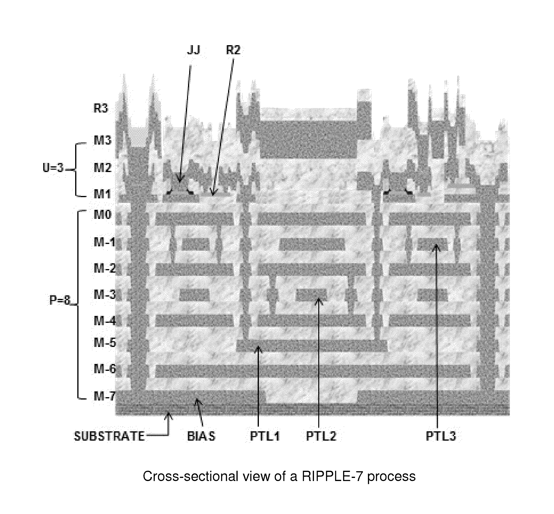
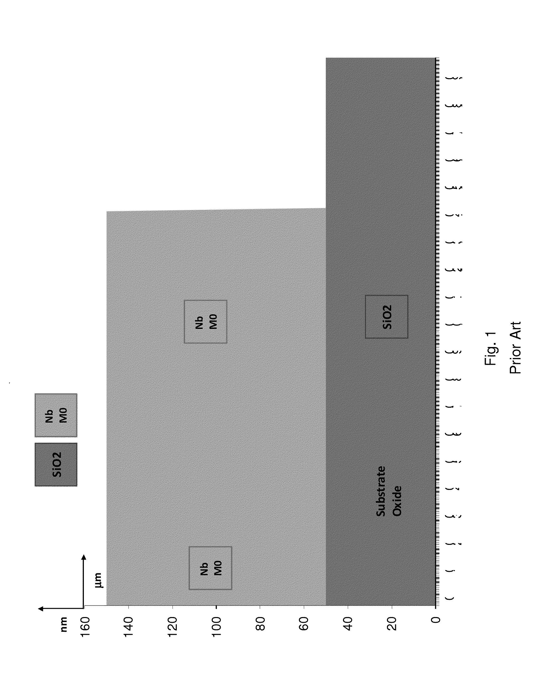
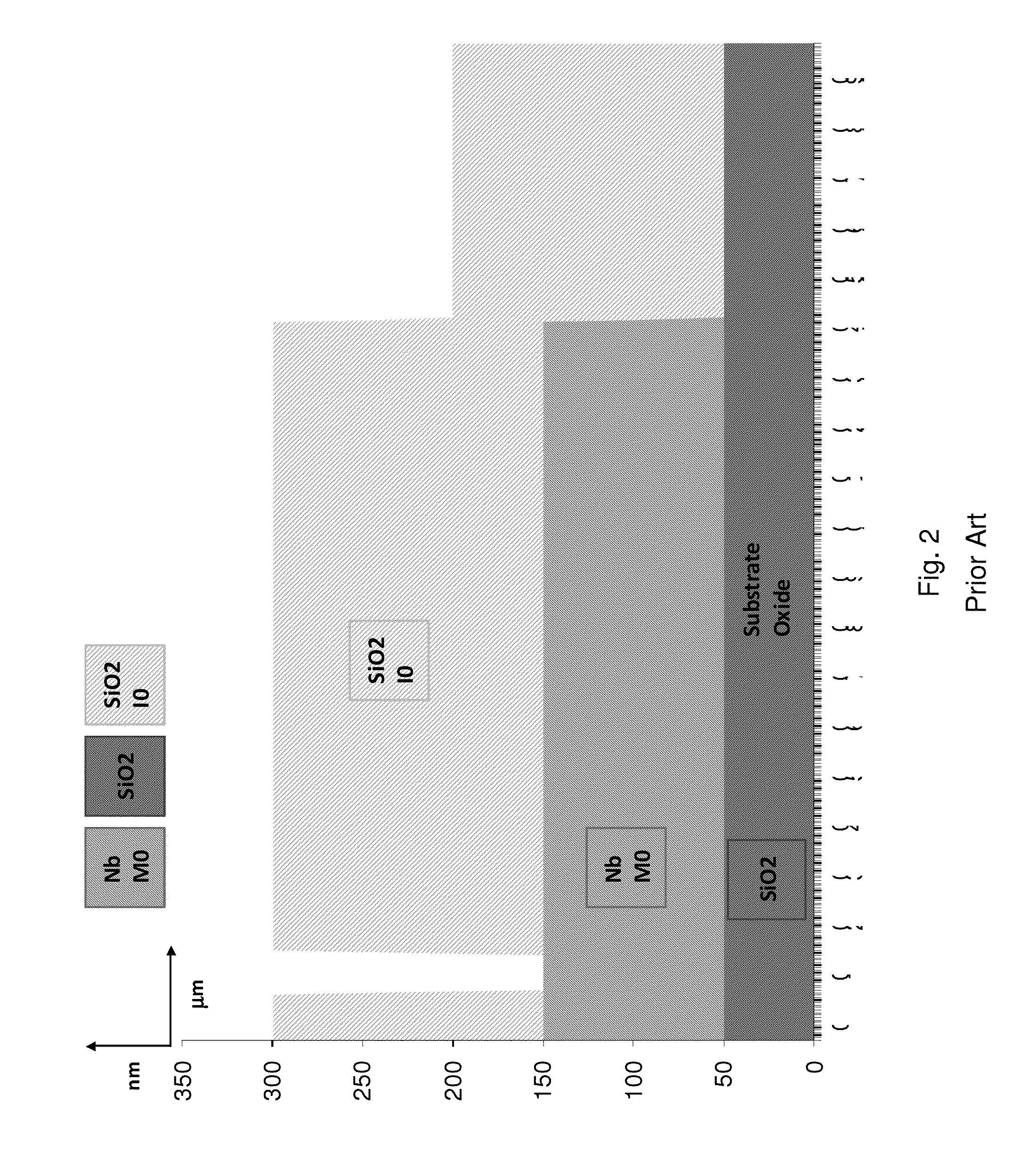
1.0 Prior Art Fabrication Process

[0123]The details of a known Hypres Inc. (Elmsford N.Y.) the process flow will be described by following the cross-section of a biased, shunted Josephson junction as it made layer-by-layer. The layout of this is given in FIG. 12, which shows a layout of a shunted Junction connected to a bias pad with a bias resistor and grounded through the base electrode of the junction.

[0124]The process starts with a bare 150 mm diameter oxidized silicon wafer by deposition the first Nb metal layer (M0). Of course, other substrates may be used. Typically, the substrate is planarized before the first step, and indeed, may be a planarized circuit formed from preceding manufacturing steps.

[0125]The deposition is done in a cryo-pumped chamber to a pressure of about 10−7 Torr. Magnetron sputtering is used for deposition, where the wafer is scanned under the target at constant speed. Both the scan speed and the chamber pressure are adjusted to get the required film thick...


PUM


Abstract

A method for increasing the integration level of superconducting electronic circuits, comprising fabricating a series of planarized electrically conductive layers patterned into wiring, separated by planarized insulating layers, with vias communicating between the conductive layers. Contrary to the standard sequence of patterning from the bottom up, the pattern of vias in at least one insulating layer is formed prior to the pattern of wiring in the underlying conductive layer. This enables a reduction in the number of planarization steps, leading to a fabrication process which is faster and more reliable. In a preferred embodiment, the superconductor is niobium and the insulator is silicon dioxide. This method can provide 10 or more wiring layers in a complex integrated circuit, and is compatible with non-planarized circuits placed above the planarized wiring layers.

Description

CROSS REFERENCE TO RELATED APPLICATIONS[0001]The present application is a non-provisional of, and claims benefit of priority under 35 U.S.C. §119(e) from, U.S. Provisional Patent Application No. 61 / 887,919, filed Oct. 7, 2013, the entirety of which is expressly incorporated herein by reference.BACKGROUND OF THE INVENTION[0002]Superconducting integrated circuits (ICs) based on Josephson junctions (JJs) are capable of operation with very low power and high speed, orders of magnitude beyond those possible using conventional semiconducting circuits. Recently, superconducting single flux quantum (SFQ) circuits have progressed to even lower power versions with zero-static power dissipation (Mukhanov, U.S. Pat. No. 8,571,614; Herr, U.S. Pat. No. 7,852,106), making them highly competitive for application in next generation energy-efficient computing systems. However, the practical realization of superconducting digital circuits for high-end computing requires a significant increase in circu...

Claims


Application Information

Patent Timeline
Patent Type & Authority Applications(United States)
IPC IPC(8): H01L39/22H01L39/02H01L27/18H01L39/24
CPCH01L39/223H01L39/2406H01L27/18H01L39/025H01L39/2493G11C11/44H10N69/00H10N60/0912H10N60/12H10N60/0156H10N60/805
Inventor YOHANNES, DANIELKIRICHENKO, ALEXANDER F.VIVALDA, JOHNHUNT, RICHARD
Owner SEEQC INC
Why Eureka
Try Eureka