Array Substrate For Display Panel And Method For Manufacturing Thereof

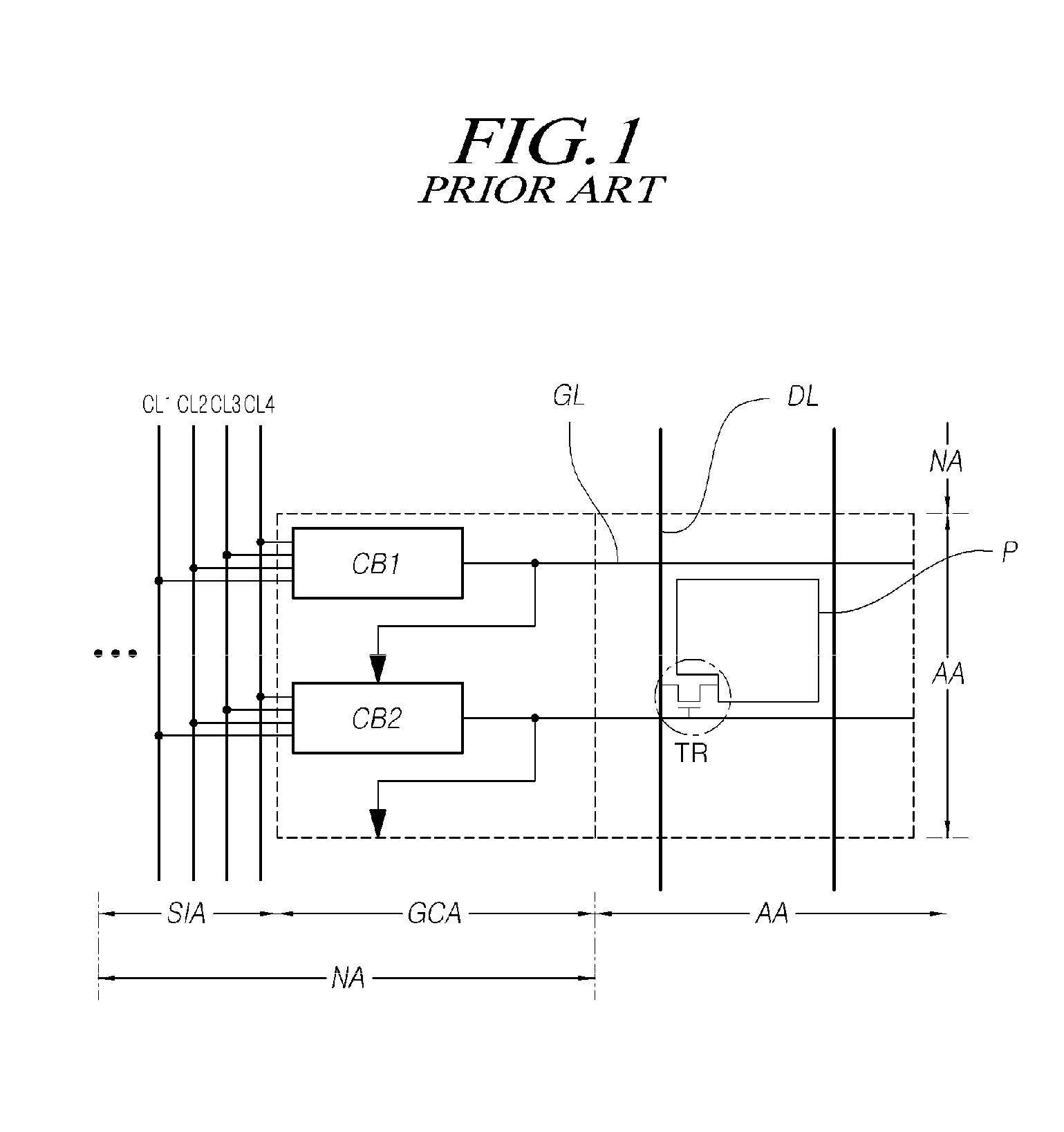
a technology of array substrate and display panel, which is applied in the direction of electrical equipment, semiconductor devices, instruments, etc., can solve the problems of static electricity generation, large quantity of electric charge stored on such signal lines, and increase in the size and weight of liquid crystal displays, so as to prevent the gate metal from being damaged

Active Publication Date: 2015-05-07
LG DISPLAY CO LTD
View PDF7 Cites 29 Cited by
  • Summary
  • Abstract
  • Description
  • Claims
  • Application Information

AI Technical Summary

Benefits of technology

[0023]Another object of the present disclosure is to provide a display panel and a display device with a GIP structure that is adapted to prevent the generation of static electricity on an electrical line such as a signal line and the like elongated from an active area of a display device with a GIP structure, and a manufacturing method thereof.
[0037]As mentioned above, various embodiments may prevent the generation of static electricity in a display device with a GIP structure.
[0038]As mentioned above, various embodiments may prevent the generation of static electricity from the elongated signal line during manufacturing the display panel with the GIP structure, thereby preventing destroying the gate metal and the like.

Problems solved by technology

However, the driving PCB, which is divided into the gate and data driving PCBs and loaded on the gate and data pad portions, causes the size and weight of the liquid crystal display to increase.
As a result, the static electricity generated in manufacturing process of patterning the signal lines and gate metal layer may destroy an insulating layer such as a gate insulating layer between the gate metal layer and source / drain metal layer so that a gate metal layer and a source / drain metal layer may be short-circuited.
That is, during manufacturing the display panel with the GIP structure, specific signal line of the GIP is formed of a metal such as the gate metal pattern and longitudinally extends over the entire panel so that the quantity of the electric charge stored on such signal line may become too large.
Therefore, the static electricity generated in manufacturing process of the signal line may damage a part of the display panel during the following manufacturing processes.

Method used


Image

  • Array Substrate For Display Panel And Method For Manufacturing Thereof
  • Array Substrate For Display Panel And Method For Manufacturing Thereof
  • Array Substrate For Display Panel And Method For Manufacturing Thereof

Examples


first embodiment

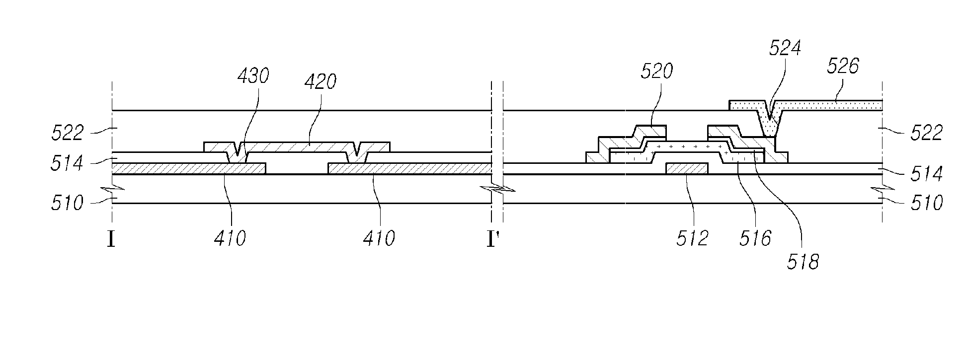
[0071]In an array substrate referring to FIGS. 4, 5 and 6A through 6C, among three embodiments described in the present specification the first line formed as a plurality of segmental lines may be formed of a gate metal and the second line may be formed of a source / drain metal, and the second line may be connected to the first line via a first contact hole formed through a gate insulating layer.

second embodiment

[0072]In an array substrate referring to FIGS. 7 and 8A through 8D, the first line may be formed of a gate metal and the second line may be formed of a pixel electrode material, and the second line may be connected to the first line via a second contact hole formed through a gate insulating layer and a passivation layer.

third embodiment

[0073]In an array substrate referring to FIGS. 9 and 10A through 10D, the second line may include a third line formed of the different layer from the first line and partially overlapped with two segmental lines of the first line adjacent to each other, and a fourth line electrically connecting the two segmental lines of the first line to the third line.

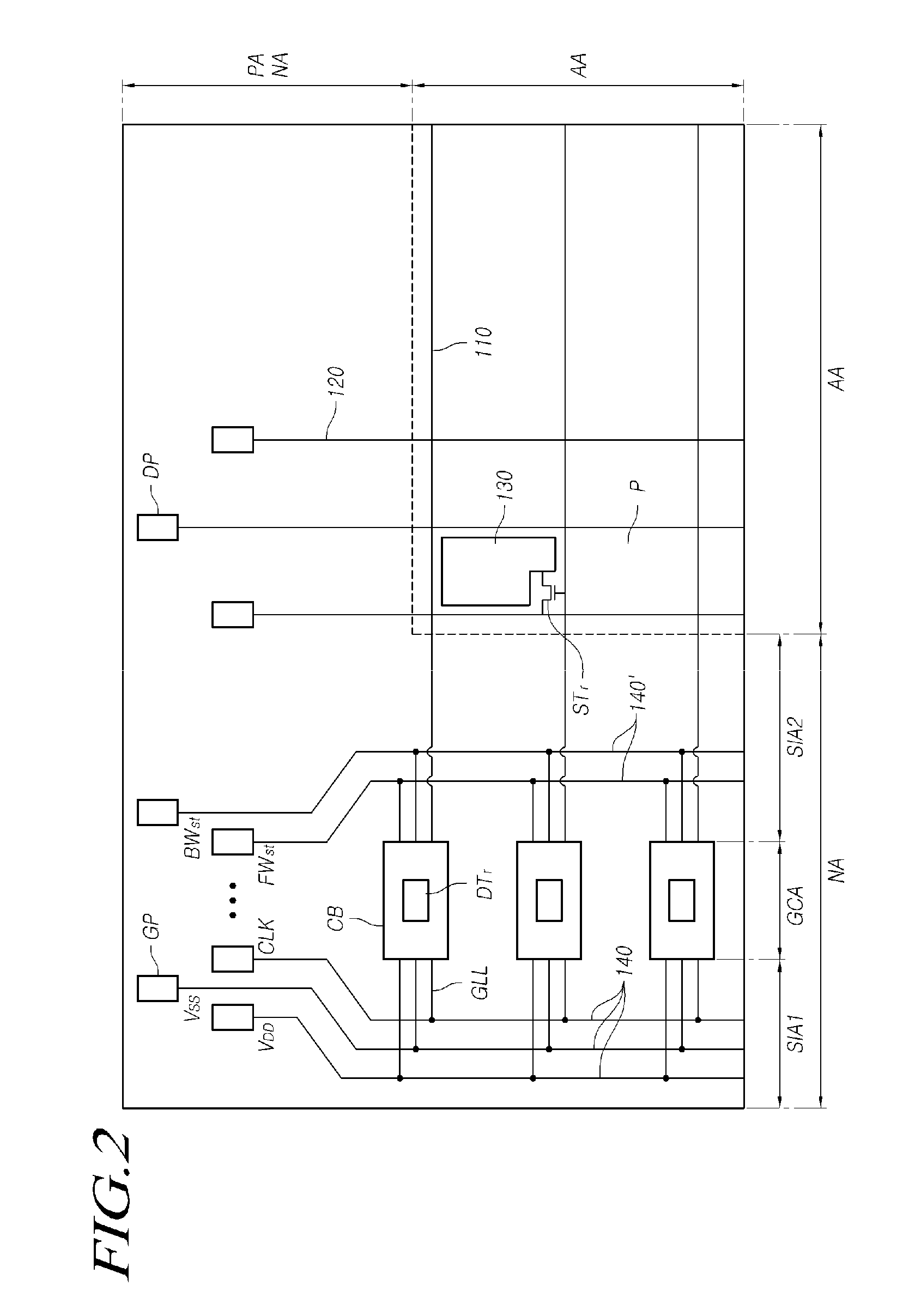
[0074]Meanwhile, although the signal line to which each of various embodiments is applied may be the start signal line disposed between the gate driving circuit and the active area, embodiments of the present disclosure are not limited thereto, but may be applied to at least one of all signal lines elongated for transferring a signal to a driving circuit on an array substrate with GIP structure, for example the VDD line, the VSS line, the CLK line and the like.

[0075]Hereafter, each of three embodiments will be described in detail in reference with the accompanying drawings.

[0076]FIGS. 4, 5 and 6A through 6C illustrate the configurati...


PUM


Abstract

Disclosed are an array substrate and a method of fabricating the same. The array substrate includes an active area including a plurality of pixels defined at an intersection area of a gate line and a data line, a gate driving circuit formed at one side of a non-active area and a signal line extending in parallel with the data line in the non-active area to transfer a signal to the gate driving circuit. The signal line includes a first line with a plurality of segmental lines, and at least one additional line formed of a different material and formed at a different layer than the first line. The at least one additional line electrically connects two segmental lines of the first line adjacent to each other.

Description

CROSS-REFERENCE TO RELATED APPLICATION[0001]This application claims priority from Korean Patent Application No. 10-2013-0134984, filed on Nov. 7, 2013, which is hereby incorporated by reference for all purposes as if fully set forth herein.BACKGROUND OF THE INVENTION[0002]1. Field of the Invention[0003]The present disclosure relates to an array substrate for a display panel and a method for manufacturing thereof. More specifically, the present disclosure relates to a structure and a method capable of preventing a damage of a substrate due to static electricity in a display panel with a gate-in-panel (GIP) structure.[0004]2. Description of the Prior Art[0005]As information oriented society has been developed, demands for displays for displaying an image are increasing. Thus, various flat displays such as a liquid crystal display (LCD), a plasma display panel (PDP), and organic light, emitting display (OLED) have been used recently.[0006]Active matrix type liquid crystal displays amon...

Claims


Application Information

Patent Timeline
Patent Type & Authority Applications(United States)
IPC IPC(8): H01L27/12
CPCH01L27/1222H01L27/1259H01L27/124G02F1/13454G02F1/136204G09G3/3677G09G2300/0408G09G2300/0426G09G2330/04G02F1/136
Inventor KIM, SOOHOKO, TAEYOUNBAE, HYUNJIKKO, INTAE
Owner LG DISPLAY CO LTD
Why Eureka
Try Eureka