Spatially resolved optical emission spectroscopy (OES) in plasma processing

a technology of optical emission spectroscopy and plasma processing, which is applied in the direction of optical radiation measurement, instruments, spectrometry/spectrophotometry/monochromators, etc., can solve the problems of large amount of acquired data, loss of all the information about local variations of plasma optical emission spectra, and thus local variations of chemical species concentration,

Active Publication Date: 2015-05-07
TOKYO ELECTRON LTD
View PDF10 Cites 15 Cited by
  • Summary
  • Abstract
  • Description
  • Claims
  • Application Information

AI Technical Summary

Problems solved by technology

Certain species, particularly transient chemical species, such as radicals have a great influence on the plasma processing outcome, and it is known that elevated local concentrations of these species can produce areas of faster processing, which may lead to nonuniformities in the processing steps and ultimately the devices being produced.
Such collection of the optical emission signal inherently results in averaging of the plasma optical emission spectra along the length of this elongated volume, also known as a ray, and thus all the inform

Method used


Image

  • Spatially resolved optical emission spectroscopy (OES) in plasma processing
  • Spatially resolved optical emission spectroscopy (OES) in plasma processing
  • Spatially resolved optical emission spectroscopy (OES) in plasma processing

Examples


Embodiment Construction

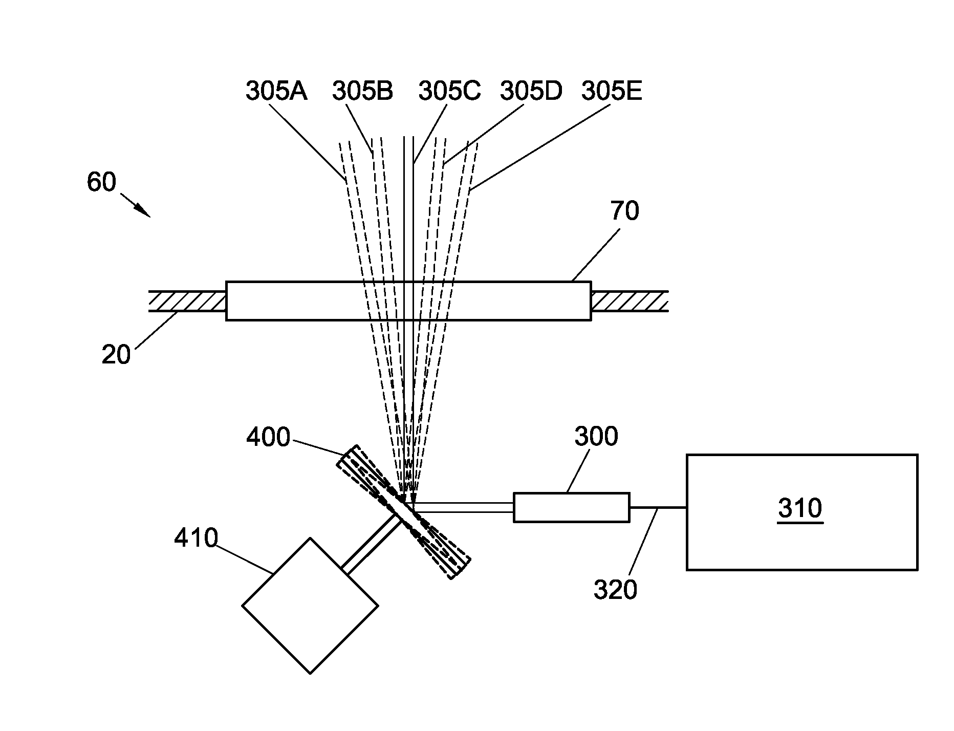
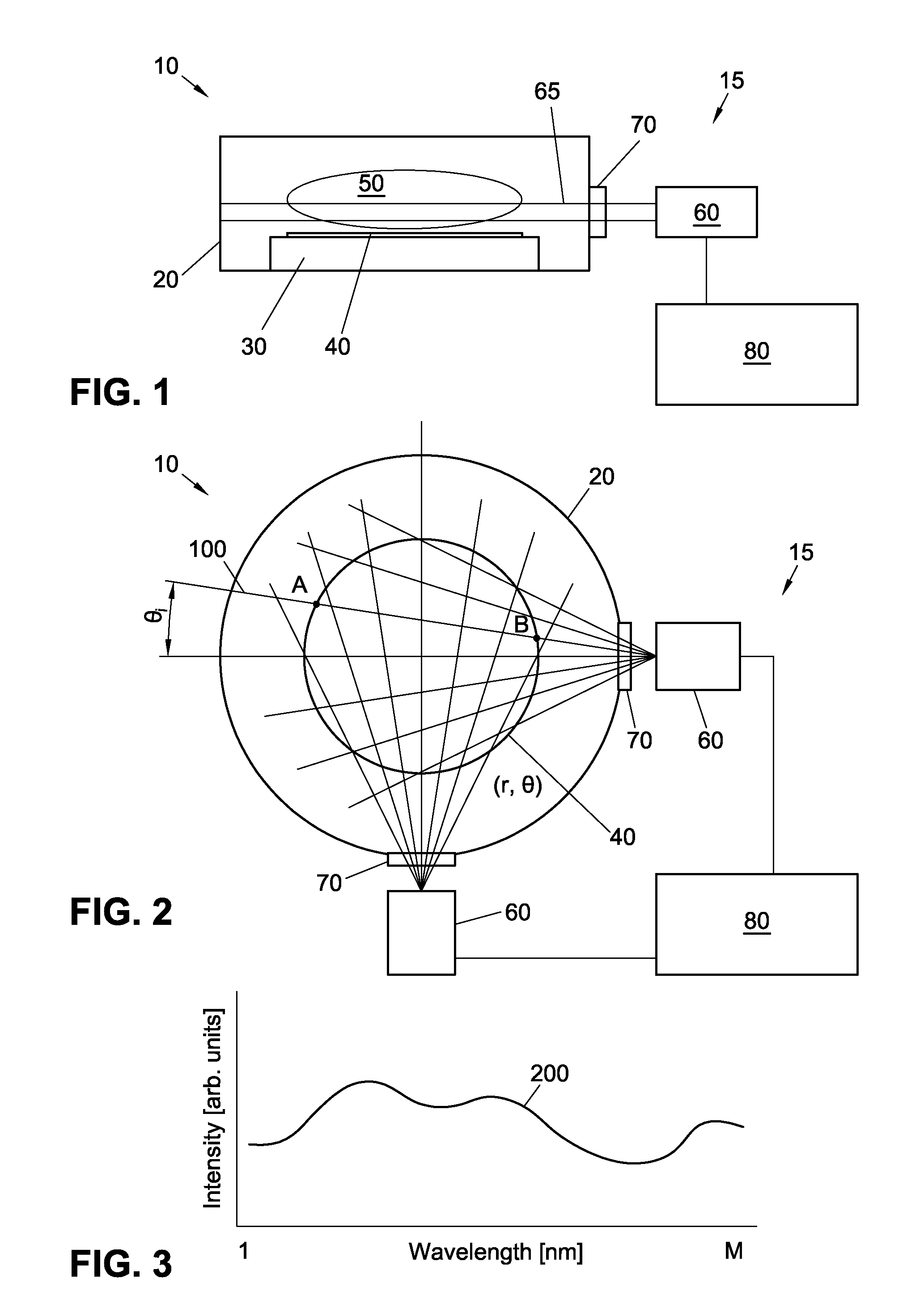
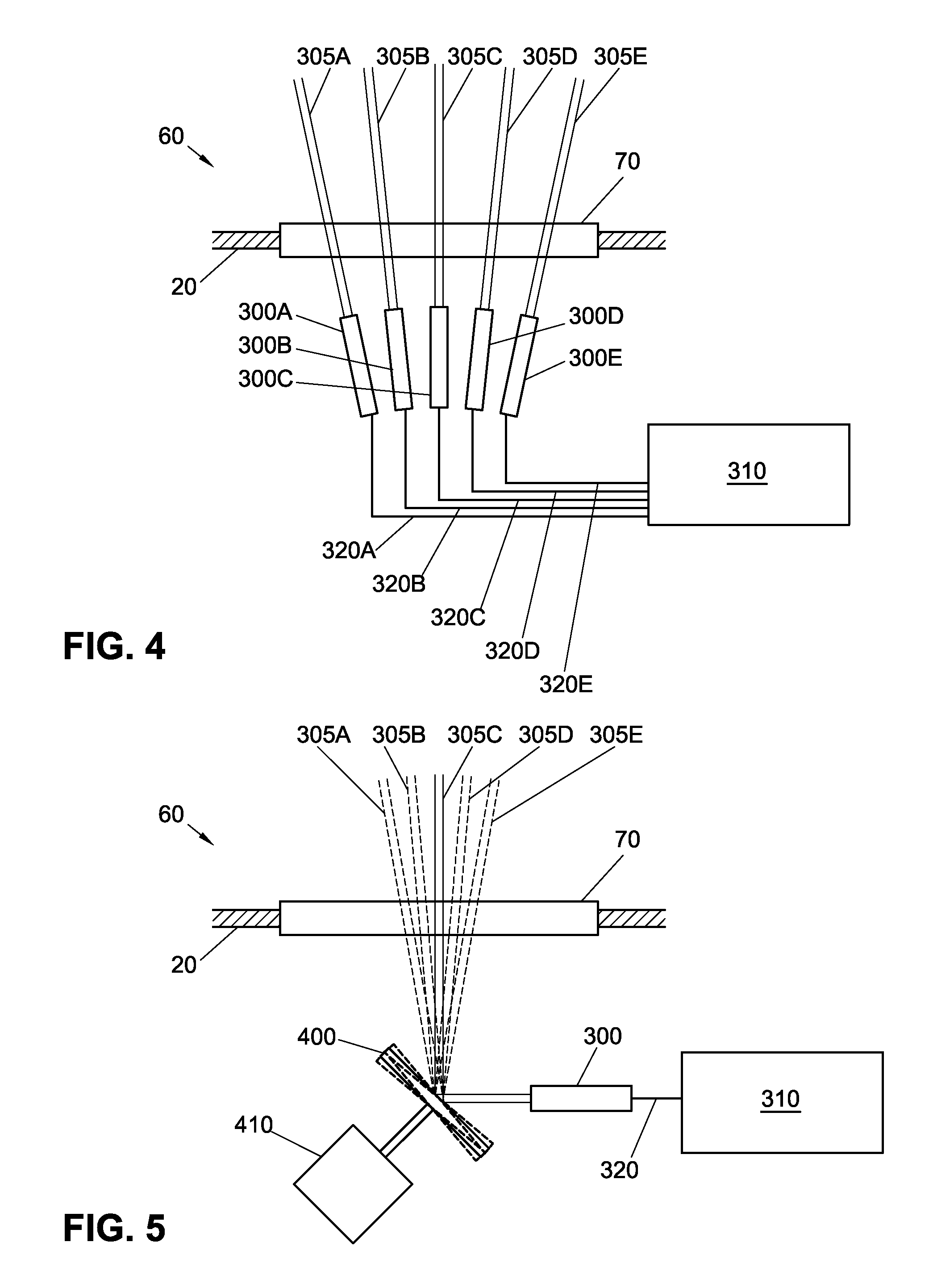
[0023]In the following description, in order to facilitate a thorough understanding of the invention and for purposes of explanation and not limitation, specific details are set forth, such as particular geometries of a plasma optical emission spectroscopy (OES) system, and descriptions of various components and processes. However, it should be understood that the invention may be practiced in other embodiments that depart from these specific details.

[0024]In the description to follow, the term substrate, which represents the workpiece being processed, may be used interchangeably with terms such as semiconductor wafer, LCD panel, light-emitting diode (LED), photovoltaic (PV) device panel, etc., the processing of all of which falls within the scope of the claimed invention.

[0025]Reference throughout this specification to “one embodiment” or “an embodiment” means that a particular feature, structure, material, or characteristic described in connection with the embodiment is included i...


PUM


Abstract

Disclosed is a method, computer method, system, and apparatus for measuring two-dimensional distributions of optical emissions from a plasma in a semiconductor plasma processing chamber. The acquired two-dimensional distributions of plasma optical emissions can be used to infer the two-dimensional distributions of concentrations of certain chemical species of interest that are present in the plasma, and thus provide a useful tool for process development and also for new and improved processing tool development. The disclosed technique is computationally simple and inexpensive, and involves the use of an expansion of the assumed optical intensity distribution into a sum of basis functions that allow for circumferential variation of optical intensity. An example of suitable basis functions are Zernike polynomials.

Description

CROSS REFERENCE TO RELATED APPLICATIONS[0001]This application is based on and claims the benefit of and priority to co-pending U.S. Provisional Patent Application No. 61 / 898,975, entitled “SPATIALLY RESOLVED OPTICAL EMISSION SPECTROSCOPY (OES) IN PLASMA ETCHING” (Ref. No. TTI-242PROV), filed on Nov. 1, 2013, the entire contents of which are herein incorporated by reference.BACKGROUND OF THE INVENTION[0002]1. Field of the Invention[0003]The present invention relates to a method, computer method, system, and apparatus for measuring concentrations of chemical species in semiconductor plasma processing using plasma optical emission spectroscopy (OES). Specifically, it relates to determining two-dimensional distributions of plasma optical emissions from which two-dimensional distributions of chemical species concentrations can be determined.[0004]2. Description of Related Art[0005]Production of semiconductor devices, displays, photovoltaics, etc., proceeds in a sequence of steps, each st...

Claims


Application Information

Patent Timeline
IPC IPC(8): G01J3/443G01N21/31
CPCG01J3/443G01N2201/10G01N21/31G01N21/68
Inventor BAO, JUNWEIMENG, CHING-LINGTUITJE, HOLGERMIHAYLOV, MIHAILCHEN, YANYAN, ZHENGZOU, HAIXINGCHU, HANYOU
Owner TOKYO ELECTRON LTD
Why Eureka
Try Eureka