
Organic material for deposition, and organic photoelectric conversion element, imaging element, deposition method, and manufacturing method for organic photoelectronic onversion element obtained using the same

Inactive Publication Date: 2015-05-14
FUJIFILM CORP
View PDF2 Cites 17 Cited by
  • Summary
  • Abstract
  • Description
  • Claims
  • Application Information

AI Technical Summary

Benefits of technology

The present invention relates to improving the manufacturing stability of an organic photoelectric conversion element. The invention aims to provide an organic material for deposition that can form an organic layer by dry deposition to achieve the photoelectric conversion element. The invention also aims to set a ratio of film purity of the organic layer obtained after the continuous dry deposition for two hours to that of the organic layer in the initial stage of deposition to 0.9 or more. Finally, the invention aims to use an organic material for deposition that does not contain the residual solvent in the content that affects the film properties upon deposition and / or in the in-plane deposited film. This results in a stable manufacturing process for the organic photoelectric conversion elements.

Problems solved by technology

In contrast, even though the high performance can be achieved, the organic photoelectric conversion element which cannot be stably manufactured is not considered to be of practical use.

Method used

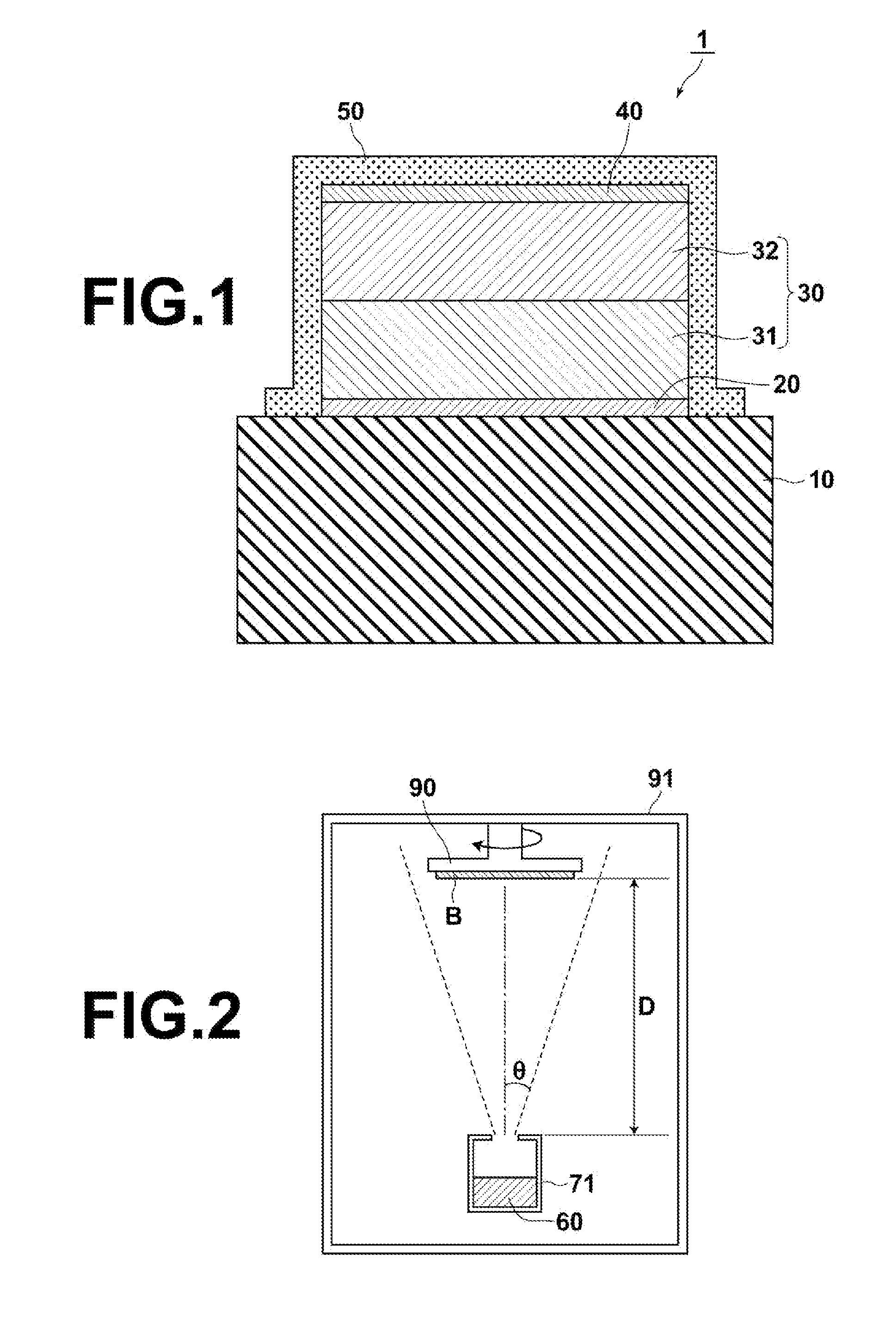
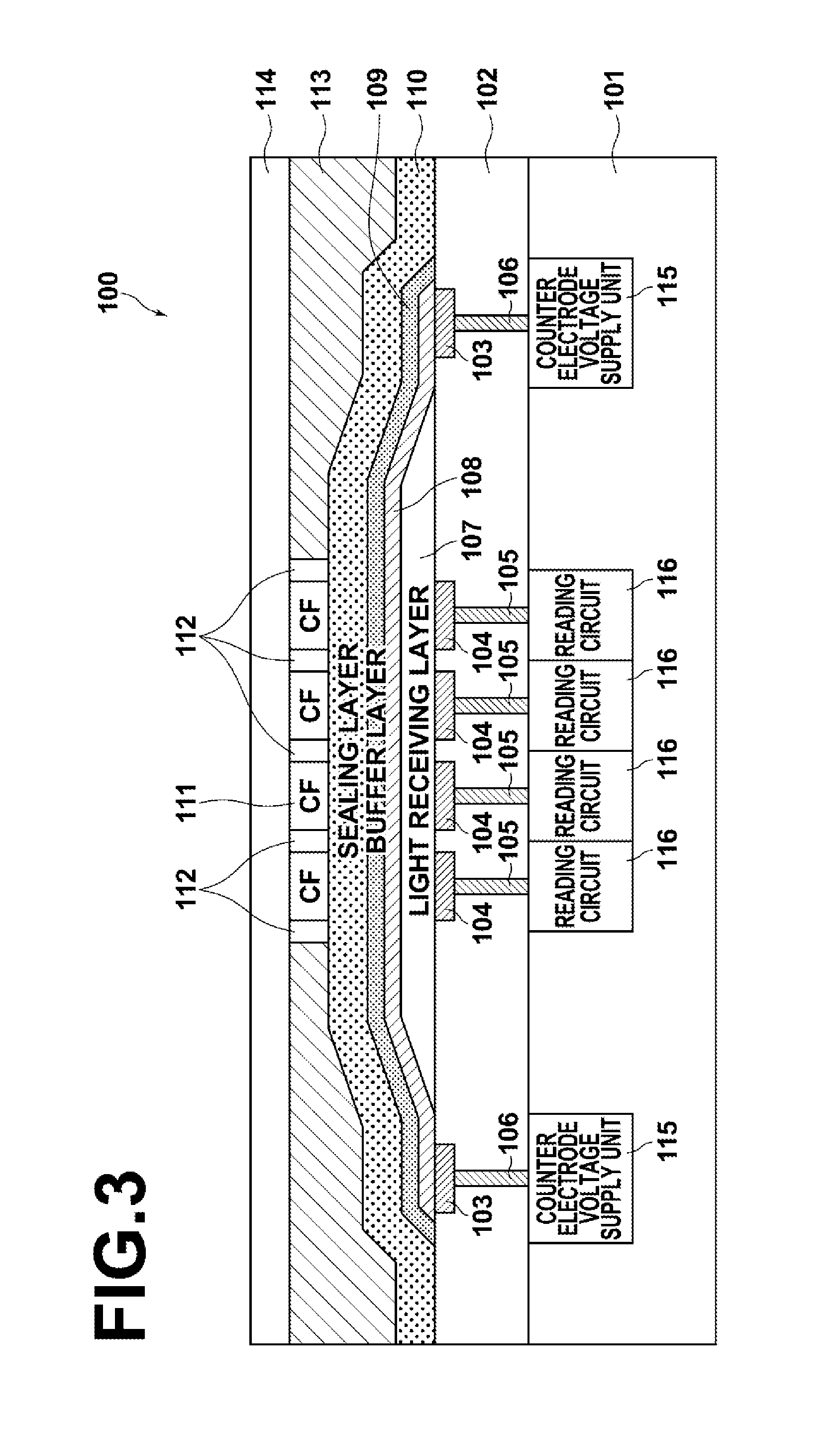
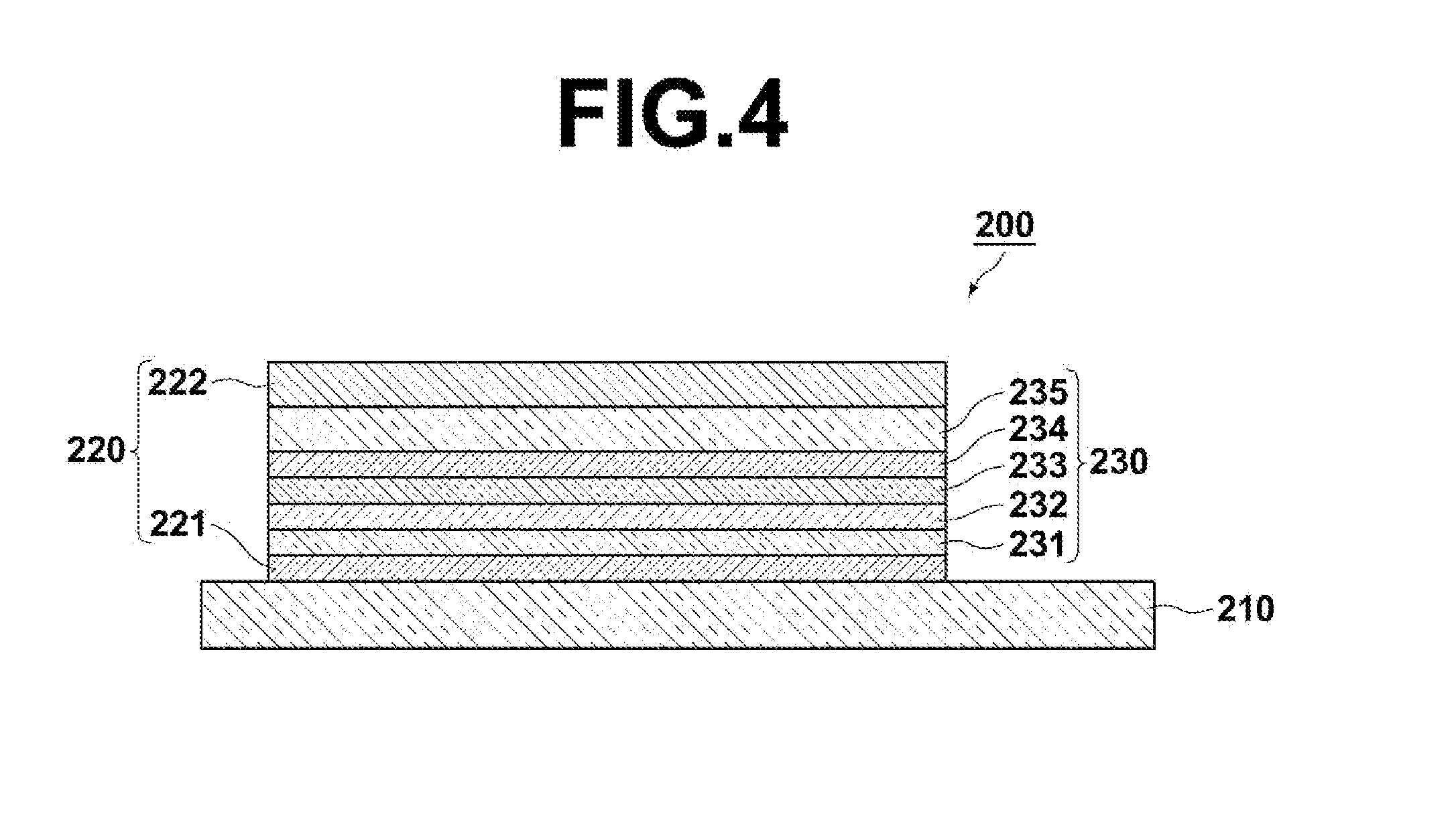

Image

  • Organic material for deposition, and organic photoelectric conversion element, imaging element, deposition method, and manufacturing method for organic photoelectronic onversion element obtained using the same
  • Organic material for deposition, and organic photoelectric conversion element, imaging element, deposition method, and manufacturing method for organic photoelectronic onversion element obtained using the same
  • Organic material for deposition, and organic photoelectric conversion element, imaging element, deposition method, and manufacturing method for organic photoelectronic onversion element obtained using the same

Examples


examples 1 to 6

, Comparative Examples 1 to 3

Synthesis of Organic Material for Deposition

[0480]First, the organic material for deposition of the above-mentioned exemplary compound 1 was synthesized. The synthesis of the exemplary compound 1 was carried out according to steps shown in the following reaction formula.

[Chemical Formula 79]

[0481]

[0482]First, 2-iso-propenyl aniline, palladium acetate, tri (t-butyl)phosphine, cesium carbonate, and 6-bromo-2-naphthoic acid methyl were dissolved in xylene, and reacted together for 5 hours under a nitrogen atmosphere at the boiling point under reflux to yield a compound 1a. The compound 1a were added into a mixture solvent of acetic acid and hydrochloric acid, and stirred for 30 minutes at 60° C. to yield a compound 1b. The compound 1b, palladium acetate, tri (t-butyl) phosphine, cesium carbonate, and bromobenzene were dissolved in xylene, and reacted for 7 hours under a nitrogen atmosphere at the boiling point under reflux to yield a compound 1c. Under the ...


PUM

PropertyMeasurementUnit
Timeaaaaaaaaaa
Pressureaaaaaaaaaa
Thicknessaaaaaaaaaa

Abstract

An organic material for deposition that is used for dry deposition of an organic layer included in an organic photoelectric conversion element is provided in which the organic material contains an organic composition of the organic layer as a principal component, and a residual solvent content of the organic material for deposition is equal to or less than 3 mol %.

Description

CROSS REFERENCE TO RELATED APPLICATIONS[0001]The present application is a Continuation of PCT International Application No. PCT / JP2013 / 004236 filed on Jul. 9, 2013, which claims priority under 35 U.S.C. §119(a) to Japanese Patent Application No. 2012-164658 filed on Jul. 25, 2012. Each of the above applications is hereby expressly incorporated by reference, in its entirety, into the present application.BACKGROUND OF THE INVENTION[0002]1. Field of the Invention[0003]The present invention relates to an organic material for deposition used for dry deposition of an organic photoelectric conversion element, and an organic photoelectric conversion element, an imaging element, and an organic electroluminescent element that are obtained using the organic material for deposition. The present invention also relates to a deposition method of an organic layer included in the organic photoelectric conversion element, and a manufacturing method for the organic photoelectric conversion element.[00...

Claims


Application Information

Patent Timeline
IPC IPC(8): H01L51/00H01L27/30H01L51/52H01L27/32H01L51/56H01L51/44
CPCH01L51/0058H01L51/56H01L51/0002H01L51/442H01L51/5234H01L27/32H01L27/307H01L51/006H01L51/0072H01L51/0087H01L51/0061H01L51/0071C07D219/14C07D221/18C07C211/54C07C211/61C07C225/24C07D471/04C07D279/26C07D209/86C07C13/72C07C15/38Y02E10/549C07F15/006C07F7/0807C07F7/0812C07F7/0816C07F7/30C09B21/00C09B23/04C09B57/00C09B57/008Y02P70/50H10K71/311H10K85/621H10K85/626H10K85/636H10K85/633H10K85/631H10K85/6574H10K85/657H10K85/346H10K30/00H10K30/30H10K85/6572H10K50/18H10K71/00H10K30/82H10K39/32H10K50/828H10K59/00H10K71/10
Inventor HAMANO, MITSUMASAFUKUZAKI, EIJI
Owner FUJIFILM CORP
Learn More