Semiconductor electrostatic discharge protection apparatus

Inactive Publication Date: 2015-05-14
UNITED MICROELECTRONICS CORP
View PDF5 Cites 13 Cited by
  • Summary
  • Abstract
  • Description
  • Claims
  • Application Information

AI Technical Summary

Benefits of technology

[0021]According to aforementioned embodiments of the present invention, a semiconductor ESD protection apparatus is provided. In one embodiment of the present invention, the semiconductor ESD protection apparatus comprises an elementary transistor with a first conductivity type formed in a substrate, a guard ring with a second conductivity type surrounding the elementary transistor and a semiconductor interval region disposed between the guard ring and the elementary transistor, wherein the semiconductor interval region is an undoped region, a doped region with the first conductivity type or a doped region with the second conductivity type that has a doping concentration substantially less than that of the well region. By the way of disposing the semiconductor interval region between the guard ring and the elementary transistor, the distance of measuring from a drain of the elementary transistor to the grounded guard ring can be enlarged, and thus the resistance between the emitter and the grounded base of the bipolar junction transistor parasitized among the elementary transistor and the substrate of the semiconductor ESD protection apparatus can be increased. As a result, leakage current pa

Problems solved by technology

Such high voltage transfer will break down the gate oxide of an input stage and cause circuit error.
However, there are still problems to the conventional GGNMOS.
As a result, the conventional GGNMOS may be easily broken down, and thus to the point of permanently failure caused by an intolerable leakage cur

Method used


Image

  • Semiconductor electrostatic discharge protection apparatus
  • Semiconductor electrostatic discharge protection apparatus
  • Semiconductor electrostatic discharge protection apparatus

Examples


Embodiment Construction

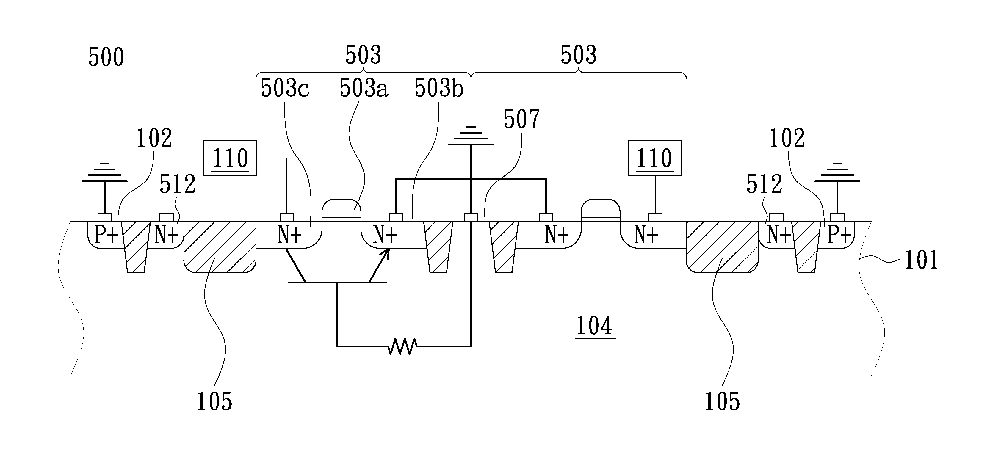
[0034]An improved semiconductor ESD protection apparatus is provided by the present invention to prevent leakage current from passing through the drain and electrically coupled to a ground reference voltage by the substrate, so as to enhance ESD tolerance of the semiconductor ESD protection apparatus from being permanent failure. In order to make the aforementioned and other objects, features and advantages of the present invention comprehensible, detail descriptions of several embodiments accompanied with figures eligible to exemplify the features of making and using the present invention are described in detail below. However, it must be appreciated that the following embodiments are just exemplary, but not be used to limit the scope of the present invention. Wherever possible, the same reference numbers are used in the drawings and the description to refer to the same or like parts.

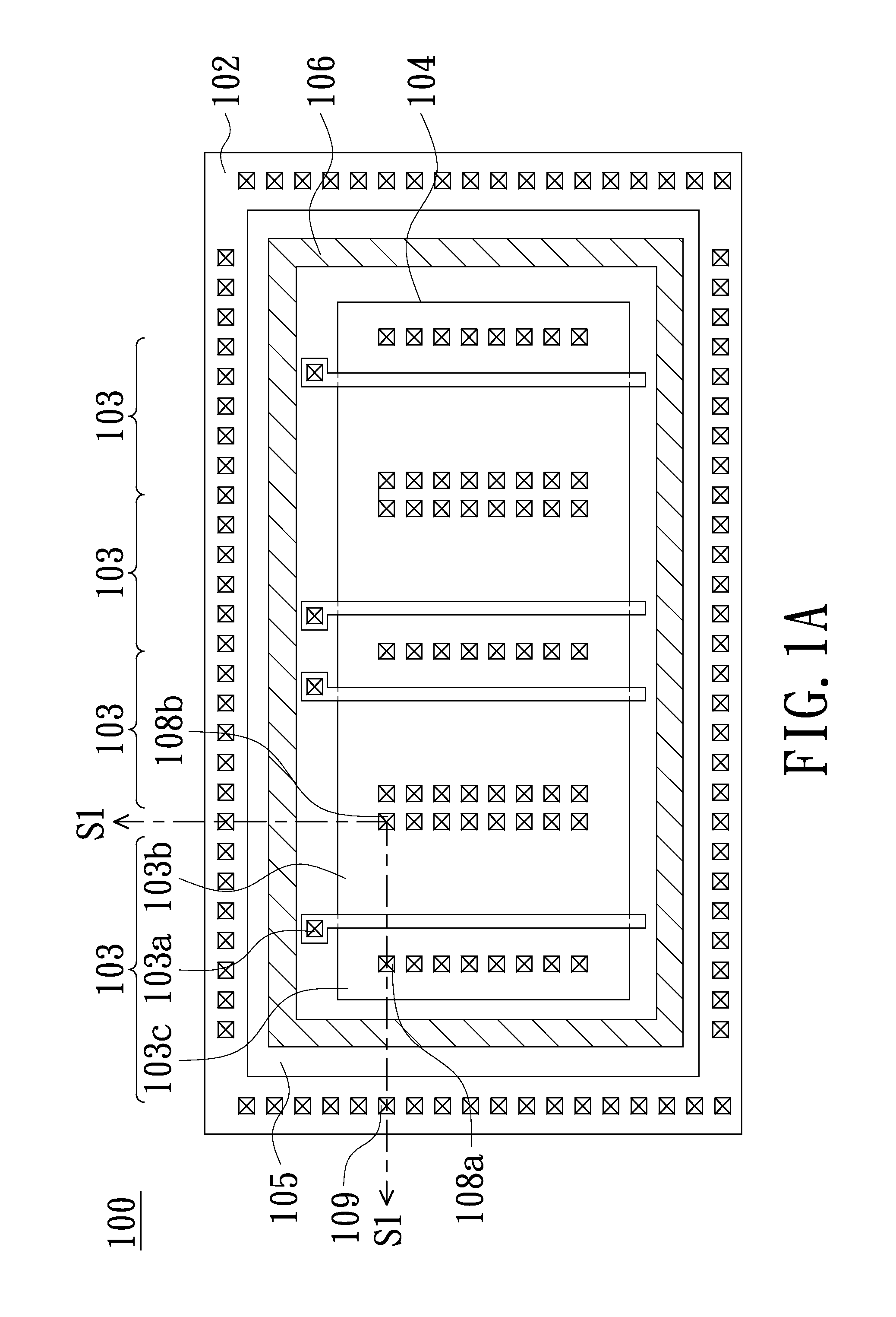
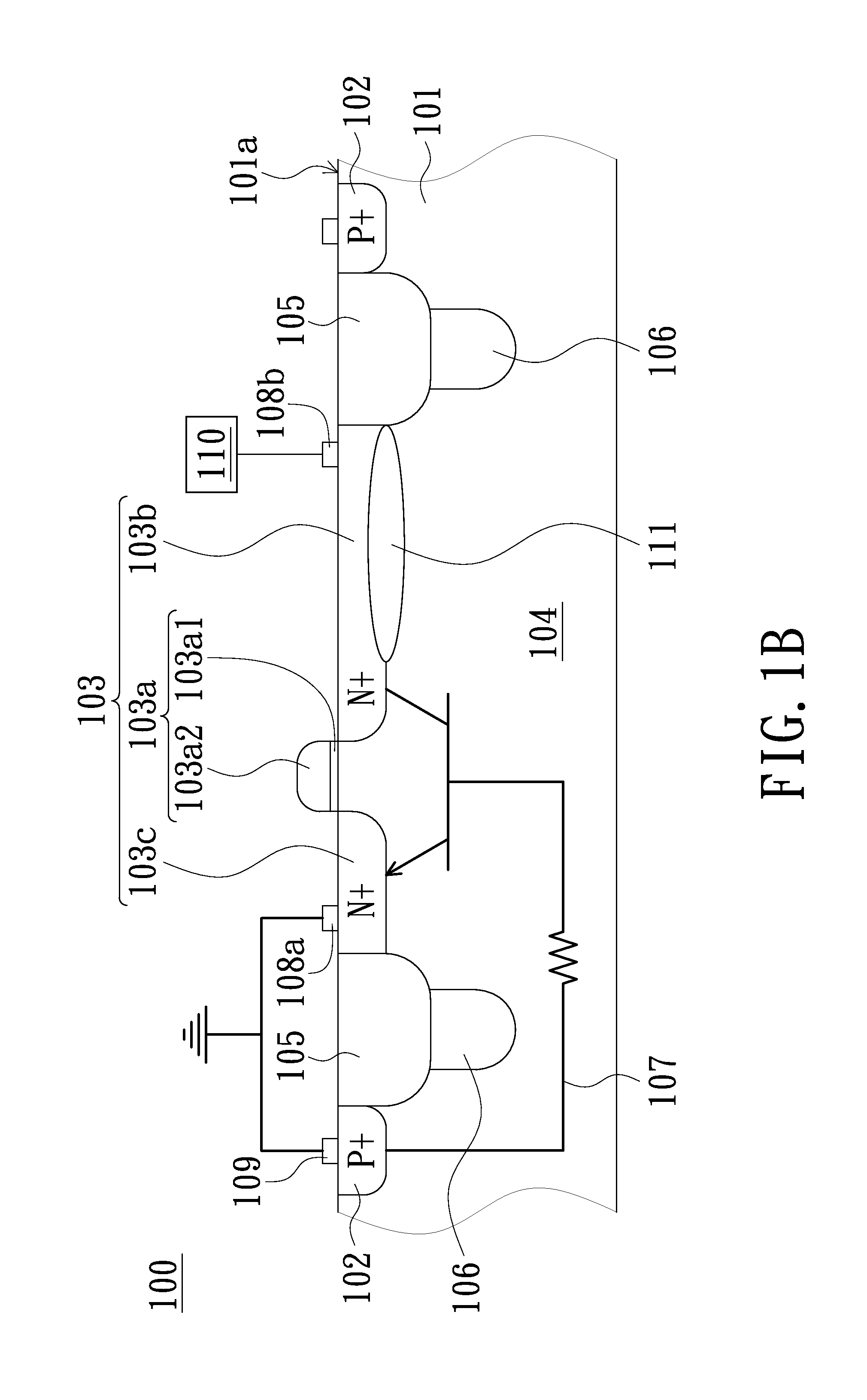
[0035]FIG. 1A is a plan view illustrating a semiconductor ESD protection apparatus 100 in accordanc...


PUM


Abstract

A semiconductor electrostatic discharge (ESD) protection apparatus comprises at least one elementary transistor with a first conductivity type, a well region with a second conductivity type, a guard ring with the second conductivity type and a semiconductor interval region. The elementary transistor is formed in the well region. The guard ring surrounds the at least one elementary transistor. The semiconductor interval region is disposed between the elementary transistor and the guard ring in order to surrounds the elementary transistor, wherein the semiconductor interval region is an undoped region, a doped region with the first conductivity type or a doped region with the second conductivity type that has a doping concentration substantially less than that of the well region.

Description

BACKGROUND OF THE INVENTION[0001]1. Field of Invention[0002]The present invention relates to a semiconductor integrated circuit (IC) device, and more particularly, relates to a semiconductor electrostatic discharge (ESD) protection apparatus.[0003]2. Description of Related Art[0004]ESD is a transient process of high energy transformation from external to internal of an IC when the IC is floated. Several hundred or even several thousand volts are transferred during ESD stress. Such high voltage transfer will break down the gate oxide of an input stage and cause circuit error. As the thickness of gate oxide is scaled down constantly, it is more and more important to provide a protected circuit or device to protect the gate oxide and to discharge ESD stress.[0005]One solution to the problem of ESD, is to provide a device for dispersing the ESD current into earth ground that is integrated into the IC. For example, a gate grounded n-type metal-oxide-semiconductor (GGNMOS) has been well k...

Claims


Application Information

Patent Timeline
IPC IPC(8): H01L27/02H01L27/088
CPCH01L27/088H01L27/0266H01L27/0277
Inventor CHEN, YU-CHUNWANG, CHANG-TZUTANG, TIEN-HAO
Owner UNITED MICROELECTRONICS CORP
Why Eureka
Try Eureka