Methods for barrier layer removal

a barrier layer and low-k dielectric technology, applied in the field of semiconductor manufacturing, can solve the problems of affecting the performance and affecting the operation of the etch process

Active Publication Date: 2015-05-21
APPLIED MATERIALS INC
View PDF1 Cites 83 Cited by
  • Summary
  • Abstract
  • Description
  • Claims
  • Application Information

AI Technical Summary

Problems solved by technology

When such demanding aspect ratios and CD control are compounded with requirements of high etch selectivity, sidewall smoothness and high tool throughput, the process window for any hardware configuration can become very small.
However, such small process windows typically suffer from performance limitations which cannot be tuned out of the etch process with known means.
Currently, low-k barrier layers are typically etched using carbon fluoride process gases; however, these carbon fluoride containing chemistries often form etching defects that degrade the structure.
These etch-related defects may affect performance and increase costs of devices that include such structures.

Method used


Image

  • Methods for barrier layer removal
  • Methods for barrier layer removal
  • Methods for barrier layer removal

Examples


Embodiment Construction

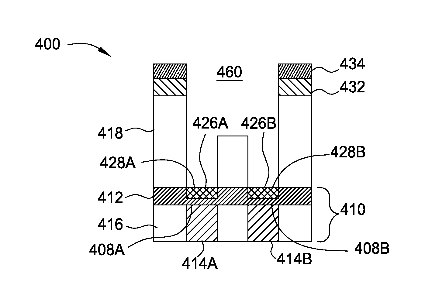
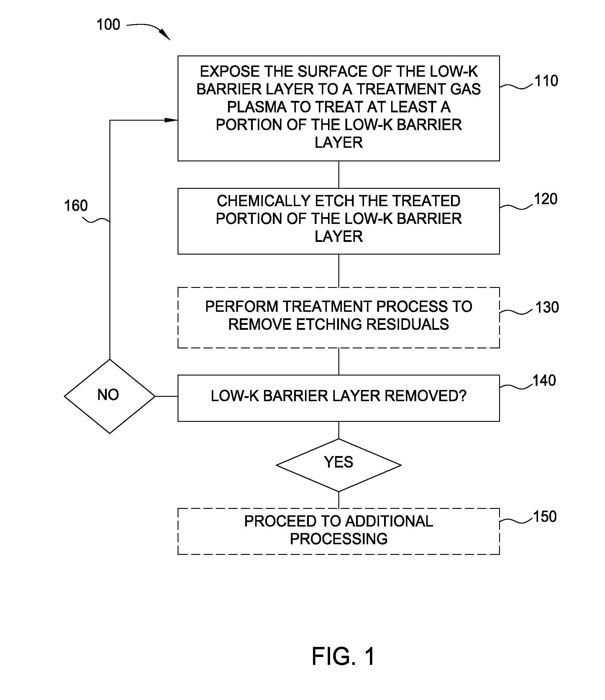
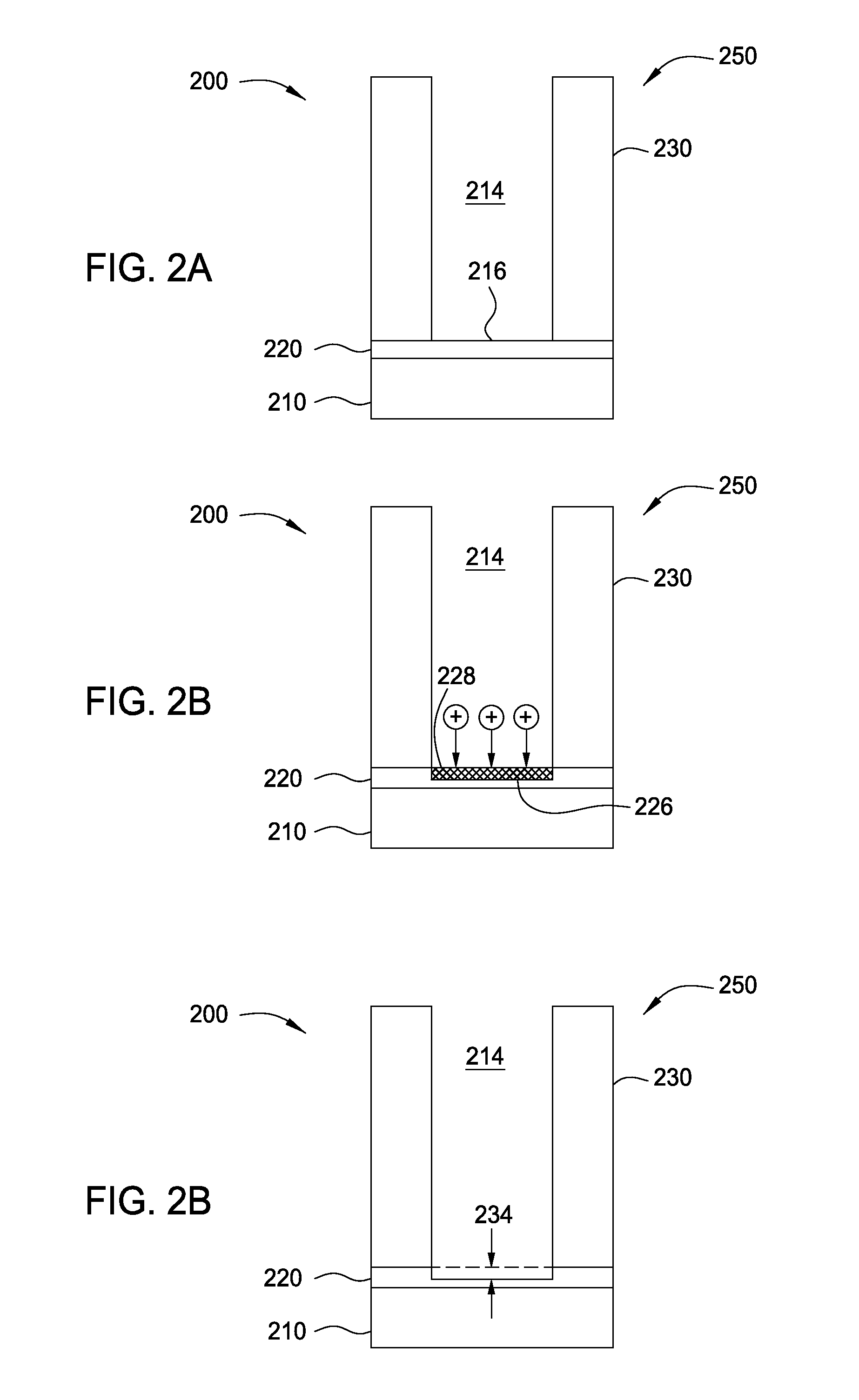
[0019]Implementations described herein generally relate to semiconductor manufacturing and more particularly to methods for etching a low-k dielectric barrier layer disposed on a substrate using a non-carbon based process. In some implementations, a new process for dual damascene formation is provided. As process dimensions continue to shrink, new schemes of etch / clean / wiring processes are needed. In conventionally known dual damascene processes, the low-k dielectric barrier layer is opened using carbon fluoride containing chemistries, followed by a wet chemical etch process to remove polymer residual formed by the carbon fluoride chemistries. The wet chemical etch process sometimes damages underlying metal films and forms etching defects that degrade the structure. However, the gap fill process is becoming more difficult due to device scaling. Thus, a new process scheme is introduced to reduce height ratios. In the dual damascene etching processes described herein, the via stops on...


PUM

PropertyMeasurementUnit
temperatureaaaaaaaaaa
diameteraaaaaaaaaa
diameteraaaaaaaaaa

Abstract

Implementations described herein generally relate to semiconductor manufacturing and more particularly to methods for etching a low-k dielectric barrier layer disposed on a substrate using a non-carbon based approach. In one implementation, a method for etching a barrier low-k layer is provided. The method comprises (a) exposing a surface of the low-k barrier layer to a treatment gas mixture to modify at least a portion of the low-k barrier layer and (b) chemically etching the modified portion of the low-k barrier layer by exposing the modified portion to a chemical etching gas mixture, wherein the chemical etching gas mixture includes at least an ammonium gas and a nitrogen trifluoride gas or at least a hydrogen gas and a nitrogen trifluoride gas.

Description

CROSS-REFERENCE TO RELATED APPLICATIONS[0001]This application claims benefit of U.S. provisional patent application Ser. No. 61 / 906,790, filed Nov. 20, 2013 and U.S. provisional patent application Ser. No. 61 / 917,236, filed Dec. 17, 2013. The aforementioned related patent applications are both incorporated by reference herein in their entirety.BACKGROUND[0002]1. Field[0003]Implementations described herein generally relate to semiconductor manufacturing and more particularly to methods for etching a low-k dielectric barrier layer disposed on a substrate using a non-carbon based approach.[0004]2. Description of the Related Art[0005]As the feature size of the device patterns get smaller, the critical dimension (CD) requirement of features becomes a more important criterion for stable and repeatable device performance. Allowable CD variation across a substrate has also scaled with the scaling of feature CD. With lateral dimensions scaling faster than vertical dimensions, because of issu...

Claims


Application Information

Patent Timeline
Patent Type & Authority Applications(United States)
IPC IPC(8): H01L21/02H01L21/311
CPCH01L21/02337H01L21/31144H01L21/31116H01J37/32449H01J37/32477H01J37/32834H01J37/32871H01L21/02063H01L21/76802H01L21/76807H01L21/76826H01L21/76829
Inventor KAO, CHIA-LINGKANG, SEANPENDER, JEREMIAH T.NEMANI, SRINIVAS D.REN, HENAIK, MEHUL
Owner APPLIED MATERIALS INC
Why Eureka
Try Eureka