Semiconductor device
a semiconductor device and reverse-conducting technology, applied in semiconductor devices, diodes, electrical apparatus, etc., can solve the problems of increasing forward voltage and steady loss, and achieve the effect of reducing snapback
- Summary
- Abstract
- Description
- Claims
- Application Information
AI Technical Summary
Benefits of technology
Problems solved by technology
Method used
Image
Examples
embodiment 1
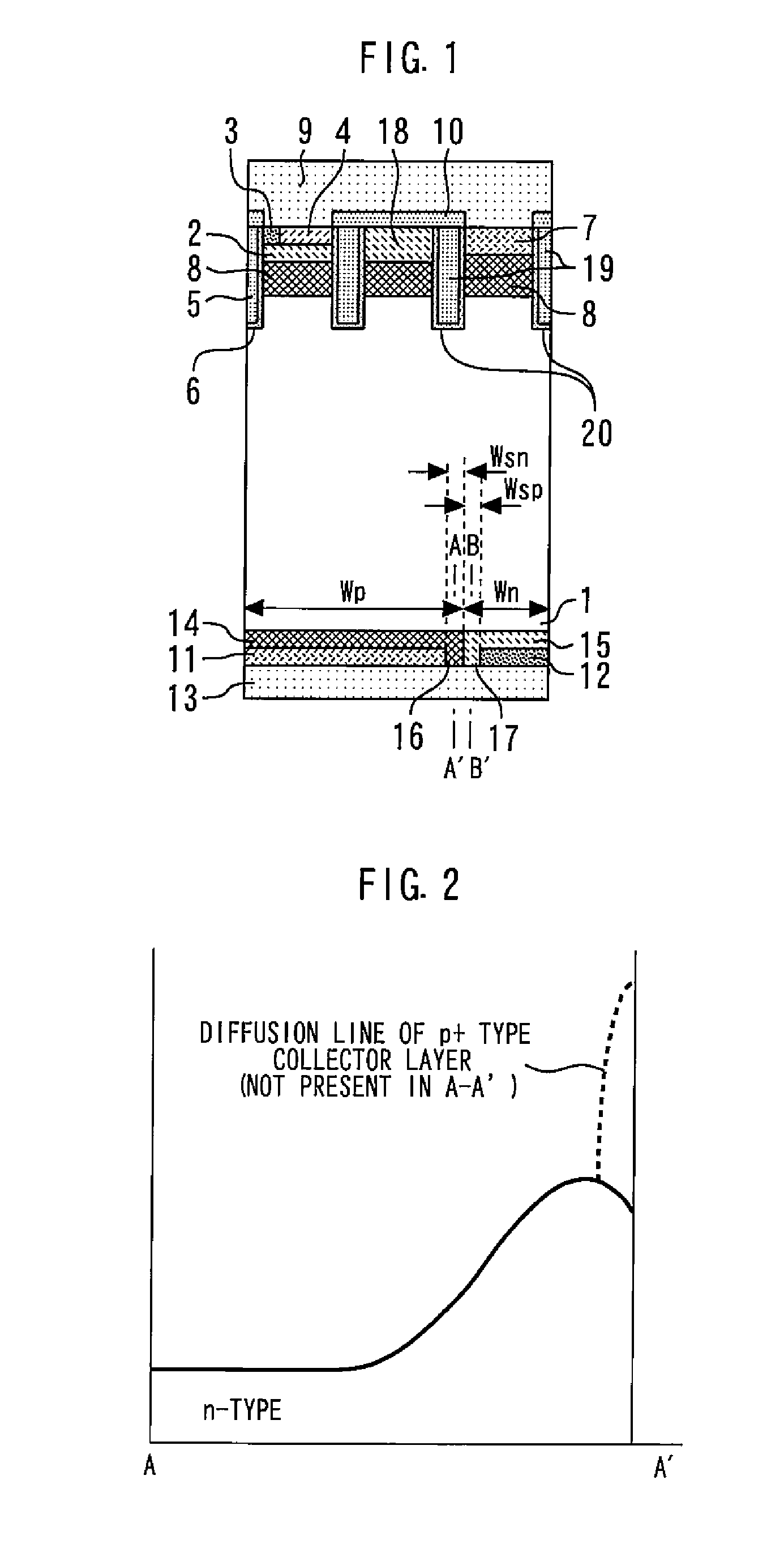
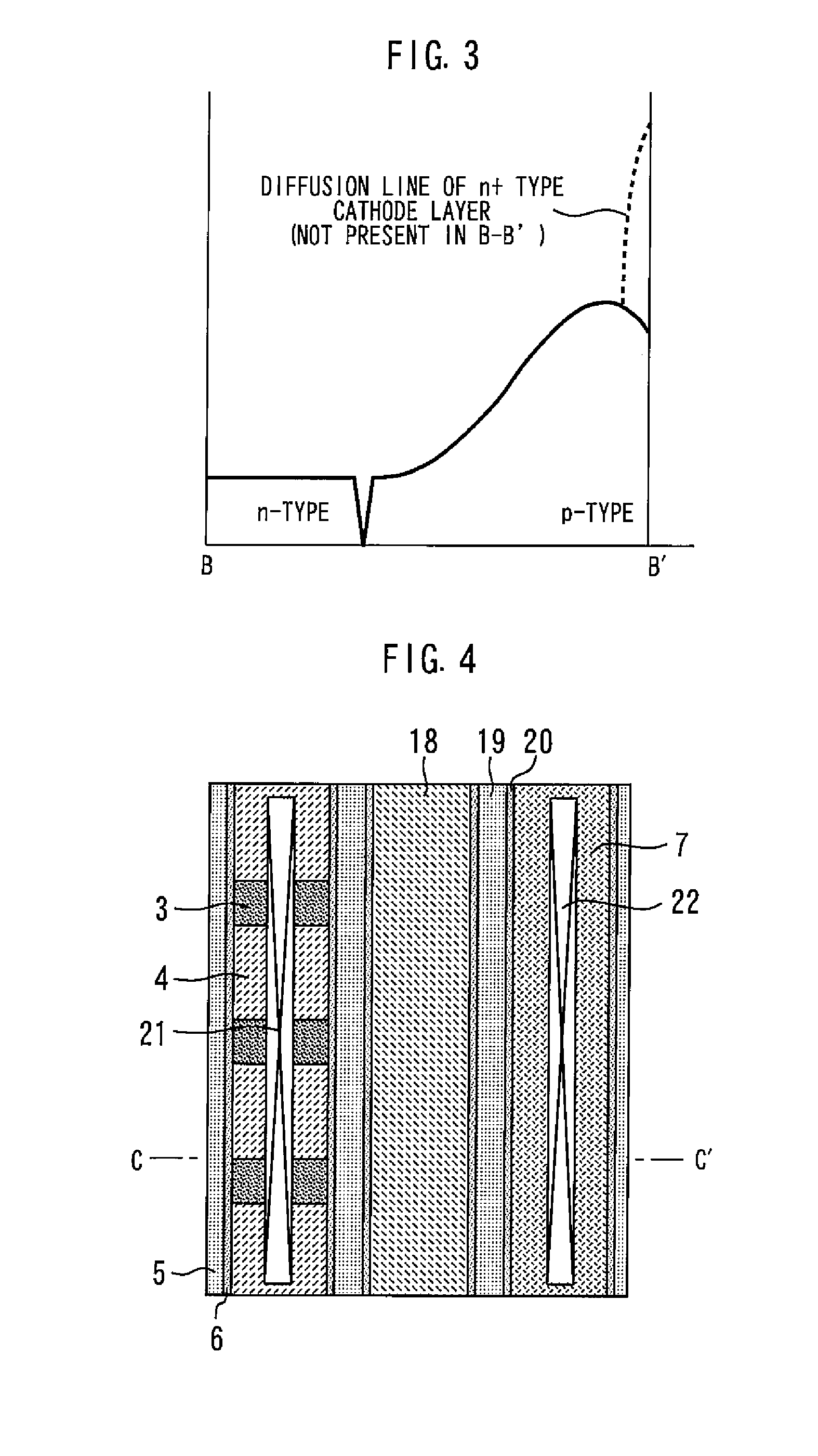
[0037]FIG. 1 is a sectional view illustrating a semiconductor device according to an embodiment 1 of the present invention. In a channel region on an n-type drift layer 1, a p-type base layer 2 is provided. On the p-type base layer 2, an n+-type emitter layer 3 and a p+-type contact layer 4 are provided. A trench-gate electrode 5 made of polysilicon penetrates the p-type base layer 2 and the n+-type emitter layer 3 and is in contact with those layers through a gate insulating film 6.
[0038]In a region other than the channel region on the n-type drift layer 1, a p-type anode layer 7 is provided. Impurity concentration of the p-type anode layer 7 is lower than the impurity concentration of the p-type base layer 2. In the p-type anode layer 7, the p+-type contact layer 4 is not formed.
[0039]Between the n-type drift layer 1 and the p-type base layer 2, an n-type carrier storing layer 8 is provided. The n-type carrier storing layer 8 is provided also below the p-type anode layer 7. An emi...
embodiment 2
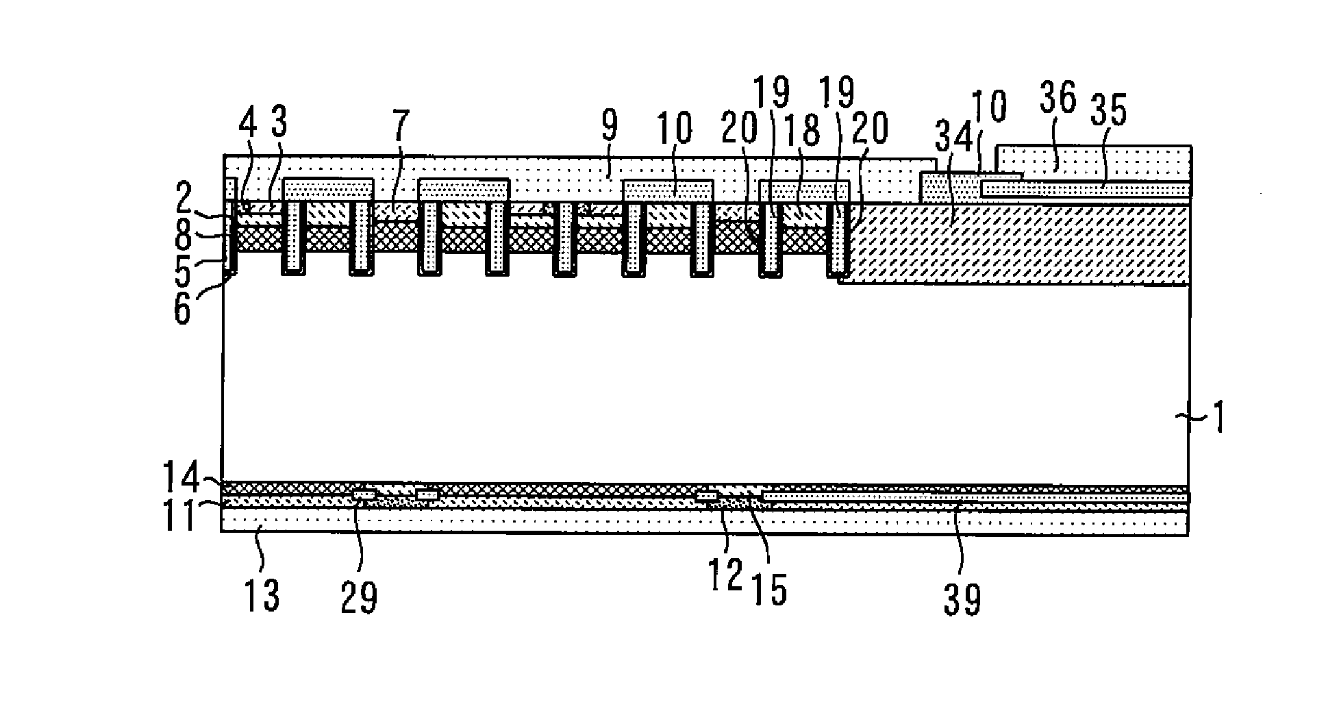
[0067]FIG. 18 is a sectional view illustrating a semiconductor device according to an embodiment 2 of the present invention. The n+-type buffer layer 14 is provided between the n-type drift layer 1 and the p+-type collector layer 11, and the p-type separation layer 15 is provided between the n-type drift layer 1 and the n+-type cathode layer 12. An embedded oxide film 29 separates the p+-type collector layer 11 and the p-type separation layer 15 from each other and separates the n+-type cathode layer 12 and the n+-type buffer layer 14 from each other.
[0068]When the embedded oxide film 29 is to be formed, first, a pattern is formed by using a general photolithography technology, and oxygen is injected to a predetermined spot by using an impurity injection technology. After the pattern is removed, by applying heat treatment, the embedded oxide film 29 is formed. The other structures can be formed by using the manufacturing method similar to the embodiment 1.
[0069]Subsequently, an oper...
embodiment 3
[0072]FIG. 19 is a sectional view illustrating a semiconductor device according to an embodiment 3 of the present invention. There is no n-type carrier storing layer 8 in this embodiment. By eliminating the n-type carrier storing layer 8, injection of the positive holes can be increased, and snapback during the FWD operation can be particularly reduced. Particularly if a repetition interval of the surface structure is short, an effect of realizing reduction of snapback and reduction of the recovery current at the same time is high.
PUM
 Abstract
Description
Claims
Application Information


