Low energy electron beam lithography

a low-energy, electron beam technology, applied in the direction of printers, instruments, electric discharge tubes, etc., can solve the problems of low throughput of such use, limited use to custom circuits made in small runs and sold at very high prices, and relatively high cost of electron beam exposure systems, so as to achieve the effect of minimizing image placement errors

a low-energy, electron beam technology, applied in the direction of printers, instruments, electric discharge tubes, etc., can solve the problems of low throughput of such use, limited use to custom circuits made in small runs and sold at very high prices, and relatively high cost of electron beam exposure systems, so as to achieve the effect of minimizing image placement errors

US20150146179A1Inactive Publication Date: 2015-05-28UTSUMI TAKAO

Image

  • Low energy electron beam lithography
  • Low energy electron beam lithography
  • Low energy electron beam lithography

Examples


Embodiment Construction

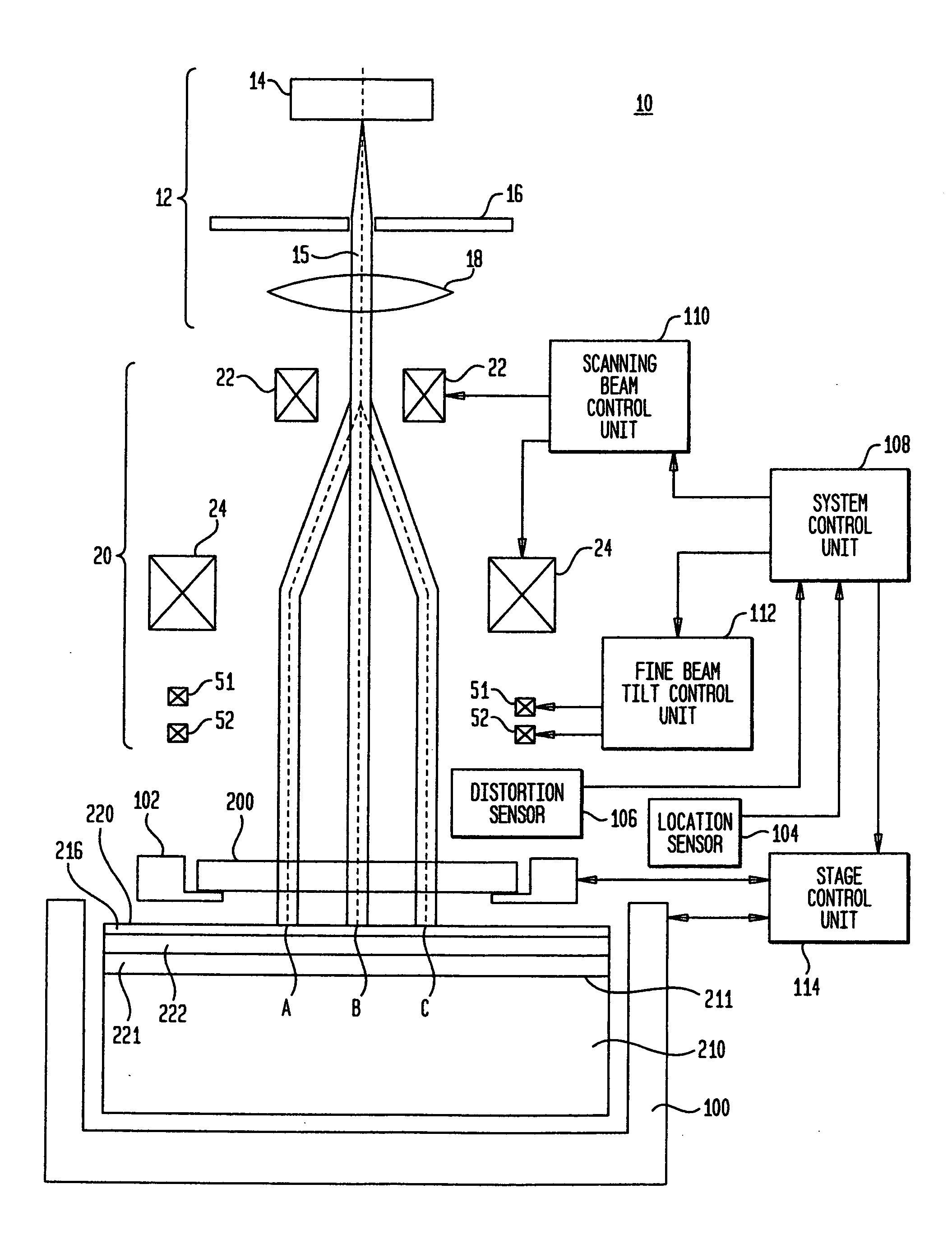
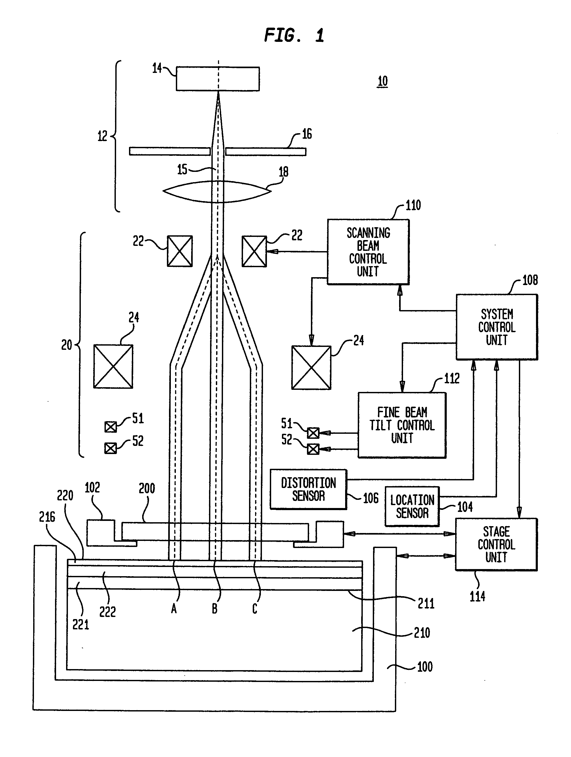
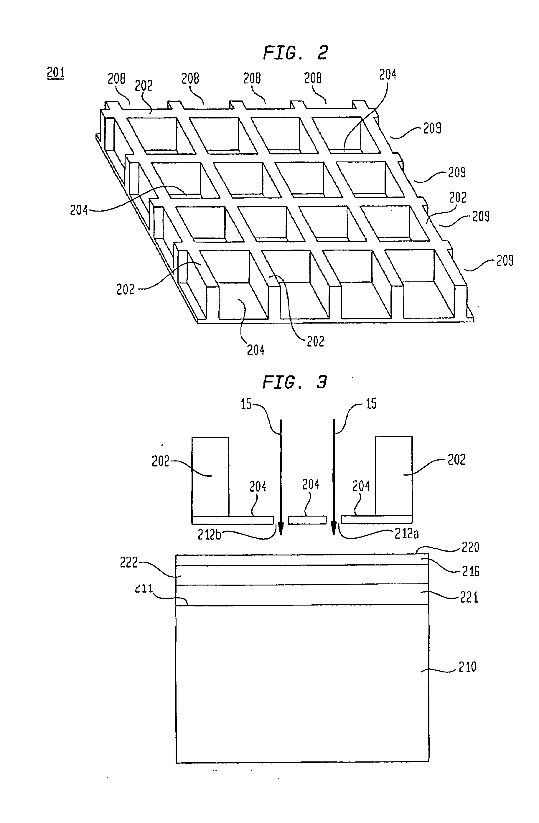
[0039]Referring now to FIG. 1, there is shown a system (electron beam apparatus) 10 in accordance with the present invention. System 10 comprises an electron gun 12 including an electron source 14 that provides abeam of electrons 15, a beam limiting aperture 16 which essentially forms a circular beam, and a condensing lens 18 that forms the electrons into an essentially parallel beam, a scanning projection system 20 including first and second main (primary) sets 22 and 24 of deflecting coils (or electrodes) for deflecting the beam as an essentially parallel beam in either a raster or a vector scan mode over and essentially normal to a surface of a mask structure 200 shown in block form. A preferred embodiment of the mask structure 200 is shown in more detail in FIGS. 2 and 3 and is denoted as an n Dimensional Complimentary Mask (nDCM). In a preferred embodiment n=4 and mask structure 200 is denoted as a 4DCM. The is an integer greater than 2. The drawing shows the electron beam 15 i...


PUM


Abstract

A low energy electron beam lithography system uses an 2 KeV electron beam of about two hundred microamperes, a 4 Division Complementary Mask (4DCM) formed from a monocrystalline silicon wafer with membranes about 100 nm thick that are surrounded by supporting silicon struts, and spaced about 50 microns from an electron sensitive resist layer about 20 nm thick that covers a nonmetallic conductive layer that covers a semiconductor wafer. Distortions in the 4DCM and semiconductor wafer are sensed and an error distortion signal is generated that results in the electron beam being tilted so as to compensate for the distortions to minimize image placement errors.

Description

FIELD OF THE INVENTION[0001]This invention relates to the manufacture of integrated circuit devices with minimum feature sizes down to about 10 nm to 20 nm, and more particularly, to apparatus and a method for use in such manufacture.BACKGROUND OF THE INVENTION[0002]A critical part of the manufacture of integrated circuit devices is the patterning of various layers on the surface of the semiconductor wafer, which after processing is diced up to provide the integrated circuit devices. These patterns define the various regions in the integrated circuit device, such as ion implantation regions, contact window regions, bonding pad regions, etc., and are generally formed by transferring patterns of geometric shapes in a mask to a thin layer of radiation resistive material, termed the ā€œresistā€, that overlies the silicon wafer within which are to be formed the integrated circuit devices. Typically the pattern on the mask is on an enlarged scale and needs to be reduced for incidence on the ...

Claims


Application Information

Patent Timeline
28 May 2015
Publication
US20150146179A1
IPC
H01L21/768
CPC
H01L21/768; H01J37/3174; H01J2237/31788
Inventors
UTSUMI, TAKAO