Copper foil and method of manufacturing the same
a technology of copper foil and manufacturing method, which is applied in the field of copper foil, can solve the problems of insufficient research on the manufacturing process, reduced flexibility and poor handling properties, and complex manufacturing process, and achieves excellent handling properties, maintain excellent appearance and color of copper-based metal materials, and improve flexibility. the effect of oxidation resistan
- Summary
- Abstract
- Description
- Claims
- Application Information
AI Technical Summary
Benefits of technology
Problems solved by technology
Method used
Image
Examples
example 1
[0069]A 0.5 mm-thick flat sheet formed of pure Cu (tough pitch copper; hereinafter, described as “TPC”) was prepared, a 0.002 um-thick cover layer formed of zinc was then formed on a surface of the flat sheet by electrolytic plating and heat treatment was subsequently performed in the ambient air at a temperature of 50° C. for 10 minutes, thereby obtaining a sample provided with a surface-treated layer. Based on Auger analysis performed on the obtained sample from the surface in a depth direction, it was confirmed that a 0.003 μm-thick surface-treated layer composed of zinc (Zn), oxygen (O) and copper (Cu) was formed.
example 2
[0070]In Example 2, a 0.5 mm-thick flat sheet formed of TPC was prepared, a 0.005 μm-thick Zn layer was then formed on a surface of the flat sheet by electrolytic plating and heat treatment was subsequently performed in the ambient air at a temperature of 50° C. for 1 hour, thereby obtaining a sample. Based on Auger analysis performed on the obtained sample from the surface in a depth direction, it was confirmed that a 0.006 μm-thick surface-treated layer composed of zinc (Zn), oxygen (O) and copper (Cu) was formed.
example 3
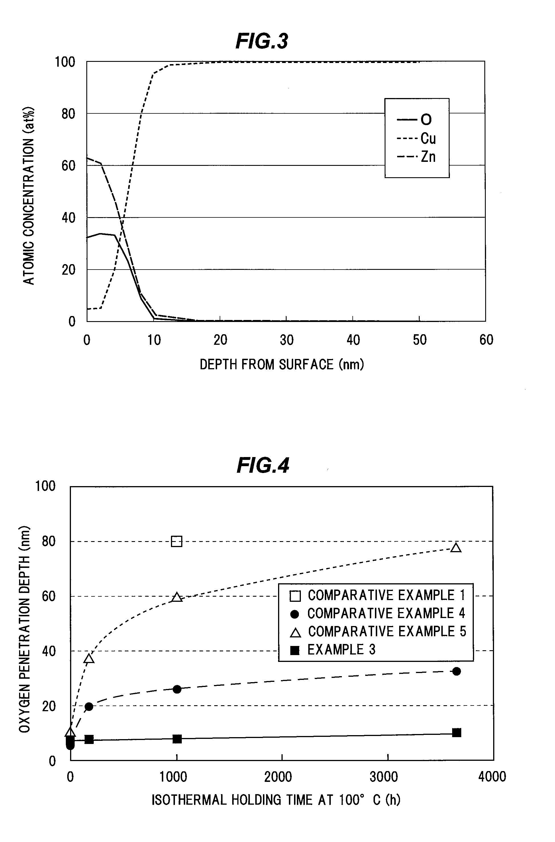
[0071]In Example 3, a 0.5 mm-thick flat sheet formed of TPC was prepared, a 0.008 μm-thick Zn layer was then formed on a surface of the flat sheet by electrolytic plating and heat treatment was subsequently performed in the ambient air at a temperature of 100° C. for 5 minutes, thereby obtaining a sample. Based on Auger analysis performed on the obtained sample from the surface in a depth direction, it was confirmed that a 0.01 μm-thick surface-treated layer composed of zinc (Zn), oxygen (O) and copper (Cu) was formed.
PUM
| Property | Measurement | Unit |
|---|---|---|
| thickness | aaaaa | aaaaa |
| thickness | aaaaa | aaaaa |
| thickness | aaaaa | aaaaa |
Abstract
Description
Claims
Application Information


