

Method for producing multicrystalline silicon substrate for solar cells
a technology of solar cells and substrates, applied in the direction of final product manufacturing, coatings, basic electric elements, etc., to achieve the effects of reducing production costs, convenient handling, and convenient washing
- Summary
- Abstract
- Description
- Claims
- Application Information
AI Technical Summary
Benefits of technology
Problems solved by technology
Method used
Image

Examples
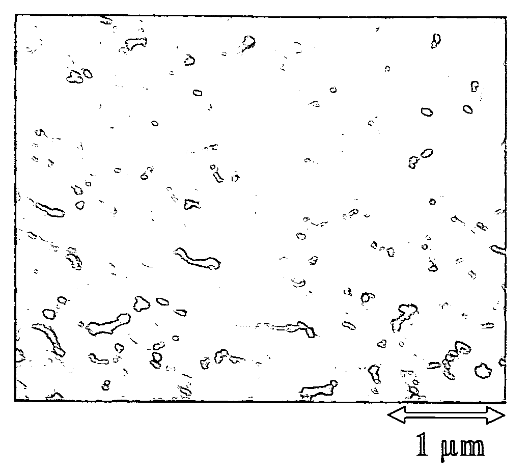
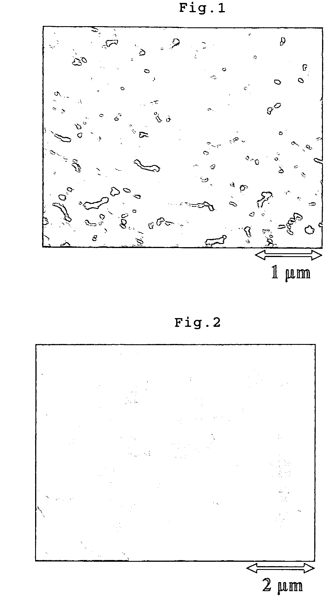
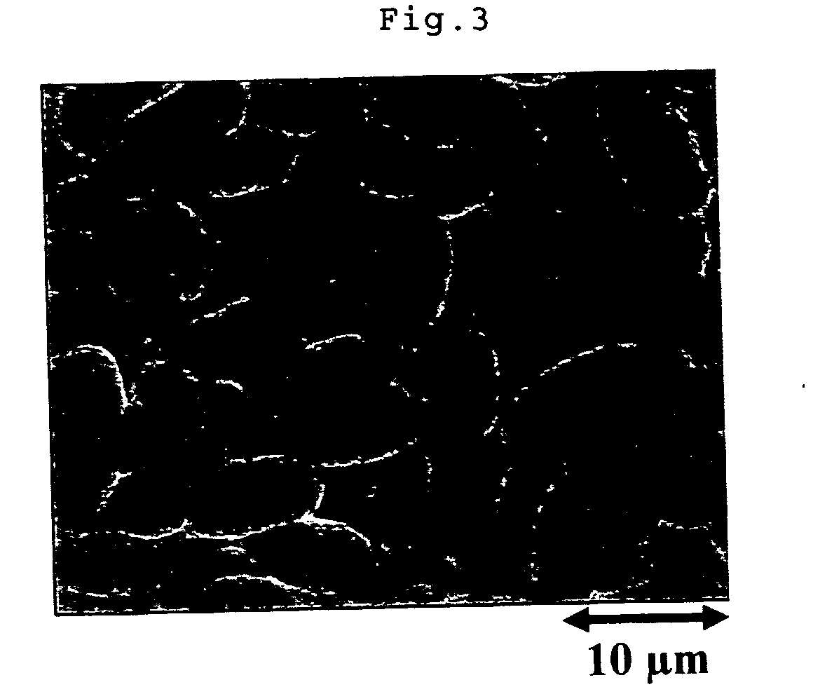
embodiment 1
[0019] The surface of a silicon substrate was textured according to the following order.
[0020] (A1) Preparation of silicon substrate: Prepared was boron-doped p-type multicrystalline silicon substrate which was thinly sliced with a mean thickness of 350 μm. The specific resistance was 0.5 to 30 cm.
[0021] (A2) Preliminary washing: The above substrate was subjected to 5 minutes of ultrasonic cleaning in acetone and then washed with pure water.
[0022] (A3) Deposition of metal particles: After the cleaning, the substrate was immersed into a 12% hydrofluoric acid solution for 2 minutes and then washed with pure water. Thereafter, it was immersed in a mixed solution of 1 mM chloroplatinic acid and 15 mM hydrofluoric acid at 40° C. for 2 minutes, and again washed with pure water.
[0023] (A4) Boring: Next, the substrate was immersed into a 12% hydrofluoric acid solution at 25° C. for 24 hours.
[0024] (A5) Removal of stain layer: After the substrate was washed with pure water, the pure wat...
embodiment 2
[0025] The surface of a silicon substrate was textured according to the following order.
[0026] (B1) Preparation of silicon substrate: Prepared was a multicrystalline silicon substrate which was the same in shape and quality as that used in Embodiment 1.
[0027] (B2) Recovery of damage: The above substrate damaged in slicing was recovered by subjecting alkaline etching by approximately 10 μm from the surface.
[0028] (B3) Preliminary washing: The substrate was immersed into a mixed solution consisting of 96% sulfuric acid and 30% hydrogen peroxide by a ratio of 1:1 for 10 minutes of washing.
[0029] (B4) Removal of oxidized film: The substrate was immersed into a 2% hydrofluoric acid solution for 1 minute to remove an oxidized film formed during Preliminary washing.
[0030] (B5) Deposition of metal particles: The substrate was immersed into an aqueous solution containing 10−4M silver perchlorate AgClO4 and 10−3M sodium hydroxide NaOH at 20 to 30° C. for 10 minutes to precipitate silver ...
PUM
| Property | Measurement | Unit |
|---|---|---|
| reflectance | aaaaa | aaaaa |
| thickness | aaaaa | aaaaa |
| diameter | aaaaa | aaaaa |
Abstract
Description
Claims
Application Information