Thin film transistor substrate having metal oxide semiconductor and manufacturing the same

a thin film transistor and metal oxide technology, applied in the direction of transistors, semiconductor devices, electrical equipment, etc., can solve the problems of degrading the video quality of the display, the pixel region may be getting larger and larger, and the horizontal electric field type lcd may have demerits, etc., to achieve good ohmic contact property and low cost

Active Publication Date: 2015-06-04
LG DISPLAY CO LTD
View PDF4 Cites 11 Cited by
  • Summary
  • Abstract
  • Description
  • Claims
  • Application Information

AI Technical Summary

Benefits of technology

[0037]According to the present invention, the thin film transistor substrate having the oxide semiconductor material has a channel area defined precisely and uniformly over the whole surface of the substrate, by forming the source-drain electrode firstly and then forming a semiconductor layer thereon. The present disclosure has a merit for suggesting a thin film transistor substrate in which the characteristics of all thin film transistors are can be optimized and stabilized over whole substrate. Further, forming a tail at under portion of the source-drain electrode using a half-tone mask process, the channel layer makes good ohmic contact property with the source-drain electrodes. In addition, using the same one half-tone mask at forming the source-drain electrode and at forming the semiconductor layer, the present disclosure suggests a method for manufacturing the thin film transistor substrate with low cost.

Problems solved by technology

However, the horizontal electric field type LCD may have demerits such as low aperture ratio and transitivity ratio of the back light.
However, when a large area display is formed in a fringe field type, the pixel region would be getting larger and the storage would be getting larger and larger.
Due to the parasitic capacitance, the video quality of the display may be degraded.
Due to this structure, there may be various problems.
In this case, if the saturation characteristics of the thin film transistor are not guaranteed, this may cause the luminance failure or distortion.
However, it is very hard to make a large area thin film transistor substrate in which all thin film transistors have almost similar size of the overlapping area OVL.

Method used


Image

  • Thin film transistor substrate having metal oxide semiconductor and manufacturing the same
  • Thin film transistor substrate having metal oxide semiconductor and manufacturing the same
  • Thin film transistor substrate having metal oxide semiconductor and manufacturing the same

Examples


first embodiment

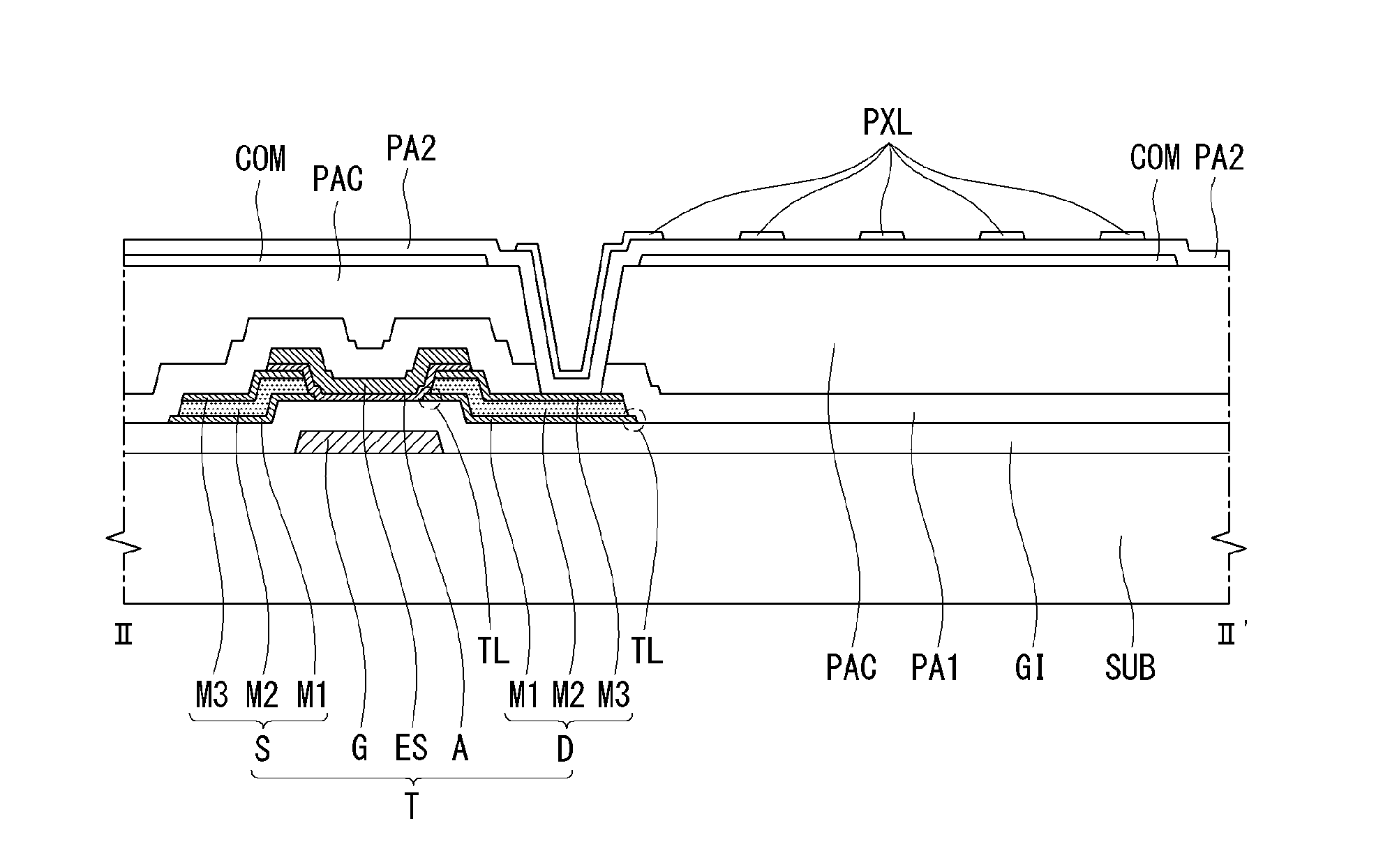
[0062]In the thin film transistor substrate according to the present disclosure, the oxide semiconductor layer A is deposited with the thickness of about 600 Å. In the case that the source-drain electrodes S and D are made of low resistance metal material such as copper or aluminum, these electrodes may be peeled off due to the bad surface contact between the copper and the IGZO. This may cause the unstable ohmic contact between the source-drain electrodes S and D and the semiconductor layer A.

[0063]As a method for addresing or minimizing the above-mentioned limitation associated with the first embodiment, referring to FIGS. 4 and 6, the second embodiment of the present disclosure will be explained. For the structure of plane view, the thin film transistor substrate according to the second embodiment is similar with that of the first embodiment. Therefore, FIG. 4 will be used as the plane view. For explaining differences, FIG. 6 shows the cross-sectional structure of the second embo...

third embodiment

[0074] the semiconductor layer A and the etch stopper ES have the same outer shape with the source-drain electrode S-D. That is, the semiconductor layer A covers and contacts the whole upper surface of the source-drain electrodes S and D. As the result, the interface contact property between the semiconductor layer A and the source-drain electrodes S and D may be enhanced.

[0075]Like this, in order to form the semiconductor layer A as having the same outer shape with the source-drain electrodes S and D, in the third embodiment, the same mask would be used. Especially, in order to form the tail TL at the first metal layer M1, it is preferable to use a half-tone mask. Hereinafter, referring to FIGS. 9A to 9K, the method for manufacturing the thin film transistor substrate according to the third embodiment will be explained. FIGS. 9A to 9K are cross-sectional views along the cutting line III-III′ in FIG. 7 for illustrating the method for manufacturing the fringe field type thin film tra...


PUM


Abstract

The present disclosure relates to a thin film transistor substrate having a metal oxide semiconductor for flat panel displays and a method for manufacturing the same. The present disclosure suggests a thin film transistor substrate including: a gate electrode on a substrate; a gate insulating layer covering the gate electrode; a source electrode overlapping with one side of the gate electrode on the gate insulating layer; a drain electrode being apart from the source electrode and overlapping with other side of the gate electrode on the gate insulating layer; an oxide semiconductor layer contacting an upper surface of the source electrode and the drain electrode, and extending from the source electrode to the drain electrode; and an etch stopper having the same shape with the oxide semiconductor layer, and contacting an upper surface of the oxide semiconductor layer.

Description

CROSS-REFERENCE TO RELATED APPLICATION[0001]This application claims priority to Patent Application No. 10-2013-0148531 filed on Dec. 2, 2013 in Republic of Korea, which is incorporated by reference herein in its entirety.BACKGROUND OF THE INVENTION[0002]1. Field of the Invention[0003]The present disclosure relates to a thin film transistor (TFT) substrate having a metal oxide semiconductor for flat panel displays and a method for manufacturing the same. Particularly, the present disclosure relates to a thin film transistor substrate and a manufacturing method the same for the flat panel display in which an oxide semiconductor material is formed after forming the source-drain electrode so that the channel area can be precisely defined.[0004]2. Discussion of the Related Art[0005]Nowadays, as the information society is developed, the requirements of displays for representing information are increasing. Accordingly, the various flat panel displays (FPDs) are developed for overcoming man...

Claims


Application Information

Patent Timeline
Patent Type & Authority Applications(United States)
IPC IPC(8): H01L27/12H01L29/45H01L29/66H01L29/786
CPCH01L27/1225H01L29/7869H01L27/1288H01L29/66969H01L29/45H01L29/41733H01L29/78696H01L29/4908H01L29/78618H01L21/02565H01L21/02639H01L21/0273H01L21/47635H01L29/42356
Inventor LEE, SUNGKEUNSONG, YONGTAEKANG, IMKUKYUN, SUNGJUNJEONG, WOOCHEOL
Owner LG DISPLAY CO LTD
Why Eureka
Try Eureka