Method of manufacturing light emitting device, and light emitting device

a technology of light emitting devices and manufacturing methods, applied in semiconductor/solid-state device manufacturing, semiconductor devices, electrical equipment, etc., can solve the problems of reducing the benefit of the difficulty of making a light emitting device into a point light source, and achieve good light extraction efficiency, and increase reflectivity

Active Publication Date: 2015-06-04
NICHIA CORP
View PDF3 Cites 21 Cited by
  • Summary
  • Abstract
  • Description
  • Claims
  • Application Information

AI Technical Summary

Benefits of technology

[0015]With the method for manufacturing a light emitting device pertaining to the present disclosure, a light emitting device can be manufactured in which there is no emission from any phosphor near the light emitting element. Consequently, a light emitting device that is good in terms of being a point light source can be manufactured.
[0016]With the light emitting device pertaining to the present disclosure, a light emitting device that is good in terms of being a point light source can be obtained by preventing emission from any phosphor near the light emitting element.
[0017]Also, a light emitting device that has good light extraction efficiency can be manufactured by increasing reflectivity near the light emitting element.
[0018]With the light emitting device pertaining to the present disclosure, a light emitting device with good light extraction efficiency can be obtained by increasing reflectivity near the light emitting element.

Problems solved by technology

The benefit of a point light source is therefore reduced, so it may be difficult to make a light emitting device into a point light source.

Method used


Image

  • Method of manufacturing light emitting device, and light emitting device
  • Method of manufacturing light emitting device, and light emitting device
  • Method of manufacturing light emitting device, and light emitting device

Examples


embodiment 1

[0029

[0030]Light Emitting Device

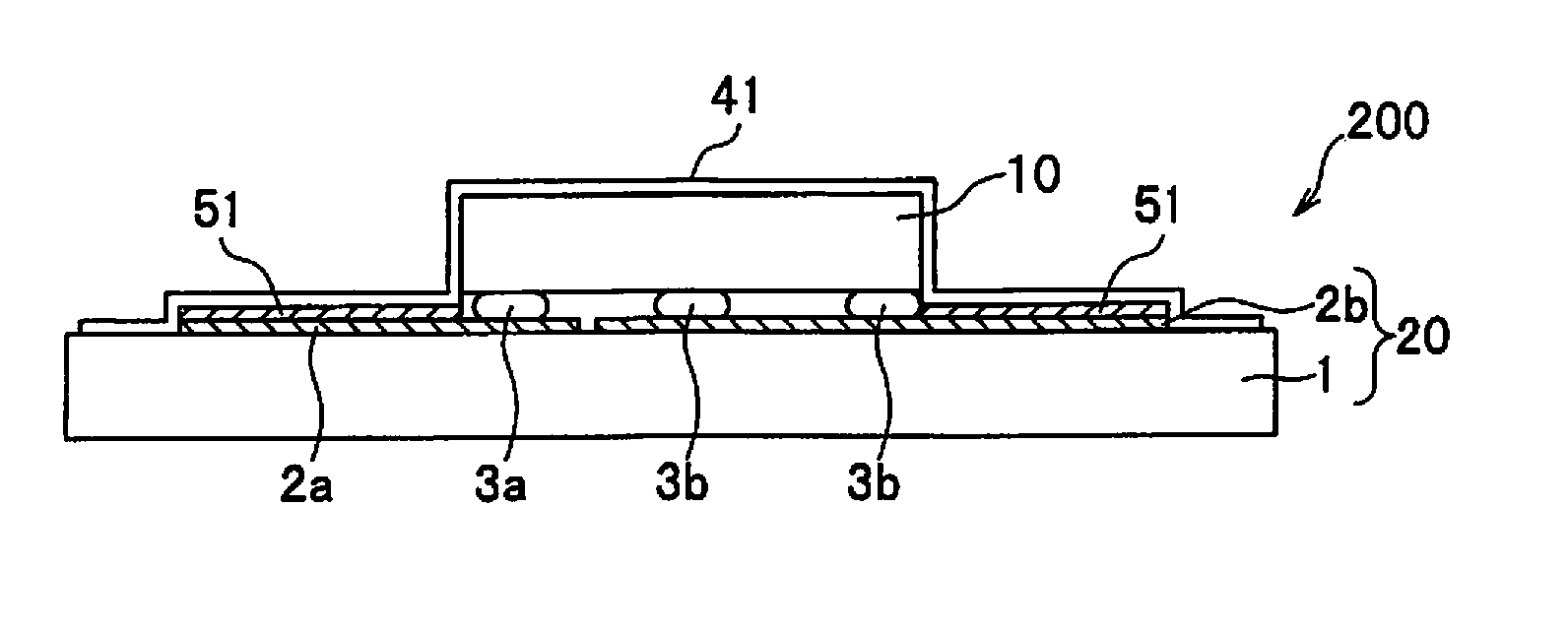
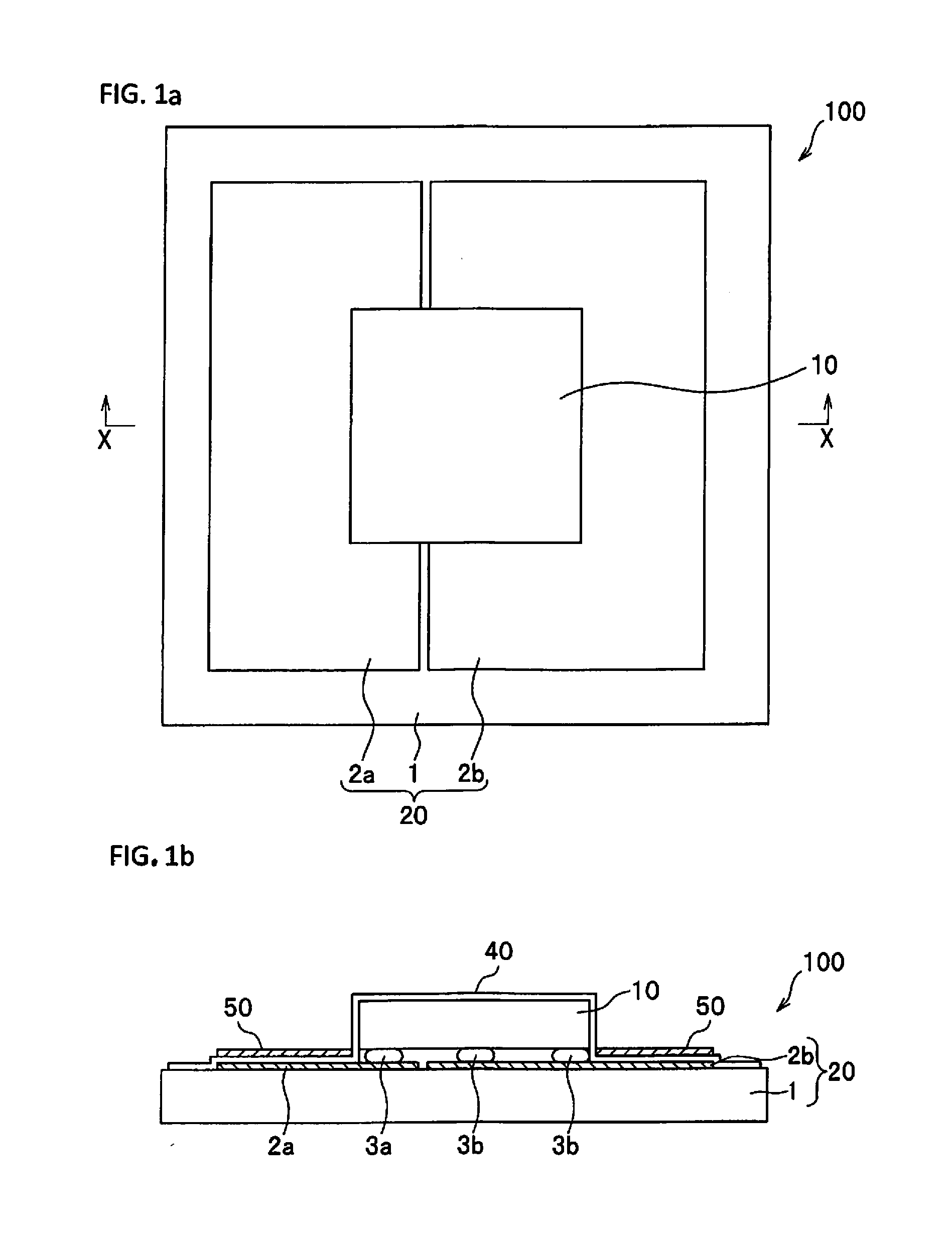
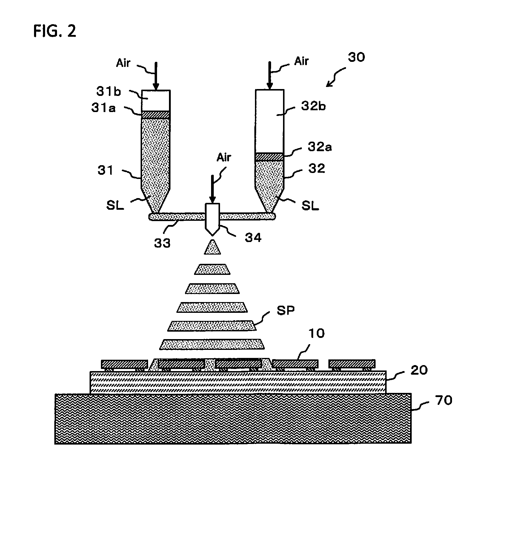
[0031]As shown in FIGS. 1a and 1b, a light emitting device 100 here mainly includes a base 1, conductive members 2a, 2b provided on the base 1, bumps 3a and 3b provided on the conductive members 2a, 3b, a light emitting element 10 provided on the bumps 3a and 3b, a phosphor layer 40 provided to the surface of the light emitting element 10 and the surface of a board (mounting board) 20, and a cover layer 50 that covers the phosphor layer 40 on the mounting board 20. The mounting board 20 here has the base 1 and the conductive members 2a, 2b. In order to facilitate an understanding of the configuration of the light emitting device of the present embodiment, the phosphor layer 40 and the cover layer 50 shown in FIG. 1b are not shown in FIG. 1a.

[0032]Mounting Board

[0033]As shown in FIGS. 1a and 1b, the mounting board 20 is a board on which the light emitting element 10 and other such electronic parts are mounted, and here includes the base 1 and the cond...

embodiment 2

[0099

[0100]As shown in FIG. 3, a light emitting device 100A is such that the conductive members 2a, 2b and the light emitting element 10 are joined by joining members 80a and 80b.

[0101]With the light emitting device 100 discussed above, the light emitting element 10 is placed on the conductive members 2a, 2b with the bumps 3a and 3b in between them. As shown in FIG. 3, however, the joining members 80a and 80b can be used to place the light emitting element 10 on the conductive members 2a, 2b by eutectic bonding or resin bonding.

[0102]Examples of the material used in eutectic bonding include alloys whose main components are gold and tin, alloys whose main components are gold and silicon, and alloys whose main components are gold and germanium. Of these, AuSn is particular preferable. The material used for resin bonding can be a resin containing a conductive material.

embodiment 3

[0103

[0104]As shown in FIGS. 4a and 4b, a light emitting device 100B has a mounting portion A on which the board (mounting board) 20 is mounted, and a groove G formed surrounding the outer periphery of the mounting portion A. The mounting board 20 here is made of the base 1 (1a, 1b, and 1c) and conductive members 2a, 3b, and 2c. The phosphor layer 40 and the cover layer 50 that are shown in FIG. 4b are not shown in FIG. 4a in order to make the configuration of the present embodiment easier to understand. The phrase “the outer periphery of the mounting portion A” here refers to an area near the light emitting element 10, which surrounds the four sides of the light emitting element 10 on the board 20, in a plan view. Also, in this embodiment, the base 1c are also located around the outer periphery of the light emitting element 10, and are included in the concept of “near the light emitting element 10.”

[0105]The light emitting device 100B thus has the groove G formed in the mounting bo...


PUM


Abstract

A method for manufacturing a light emitting device, having; a die bonding step of mounting a light emitting element on a board; a phosphor layer formation step of forming a phosphor layer that contains a phosphor by spraying on surfaces of the board and the light emitting element after the die bonding step; and a cover layer formation step of forming a cover layer that contains at least one type of light reflecting material and light blocking material on a surface of the phosphor layer over the board.

Description

CROSS-REFERENCE TO RELATED APPLICATIONS[0001]This application claims priority to Japanese Patent Applications Nos. 2013-248621 and 2014-028860 filed on Nov. 29, 2013 and Feb. 18, 2014, respectively. The entire disclosure of Japanese Patent Applications Nos. 2013-248621 and 2014-028860 is hereby incorporated herein by reference.BACKGROUND[0002]1. Technical Field[0003]The present disclosure relates to a method for manufacturing a light emitting device, and to a light emitting device, in which a phosphor layer is formed on the surface of a light emitting element.[0004]2. Related Art[0005]It is generally known that a light emitting device in which a light emitting element is used is compact, has good power efficiency, and emits light in clear colors. Since the light emitting element pertaining to this light emitting device is a semiconductor element, not only is there no worry about bulbs burning out and so forth, but the initial drive characteristics are excellent, and the device is re...

Claims


Application Information

Patent Timeline
Patent Type & Authority Applications(United States)
IPC IPC(8): H01L33/50H01L33/60H01L33/00
CPCH01L33/50H01L33/005H01L2933/0033H01L2933/0041H01L2933/0058H01L33/60H01L33/0095H01L33/54H01L33/56H01L33/62H01L2224/16225H01L2933/005
Inventor BEPPU, SUGURU
Owner NICHIA CORP
Why Eureka
Try Eureka