

High-frequency device and directional coupler
- Summary
- Abstract
- Description
- Claims
- Application Information
AI Technical Summary
Benefits of technology
Problems solved by technology
Method used
Image

Examples
first embodiment
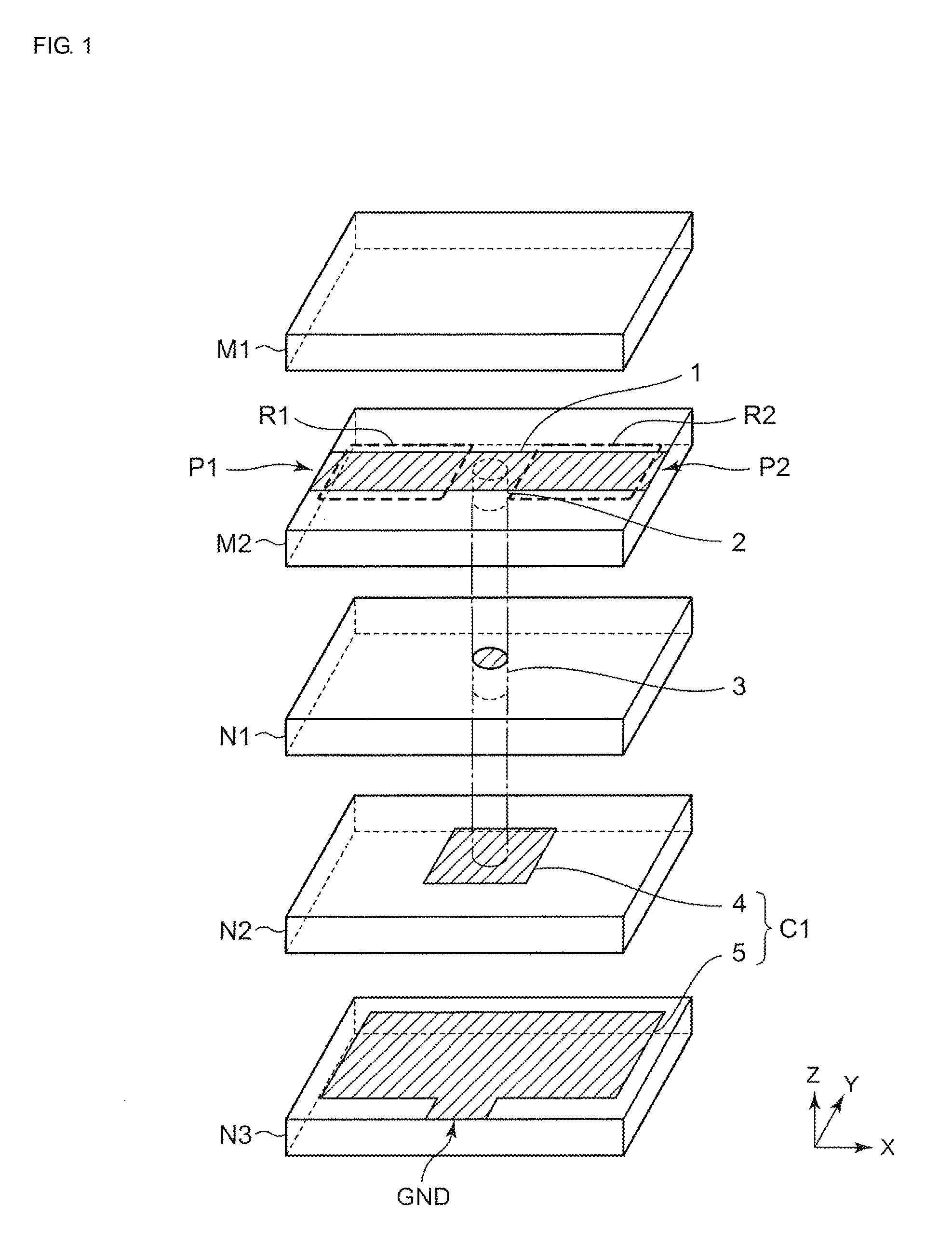
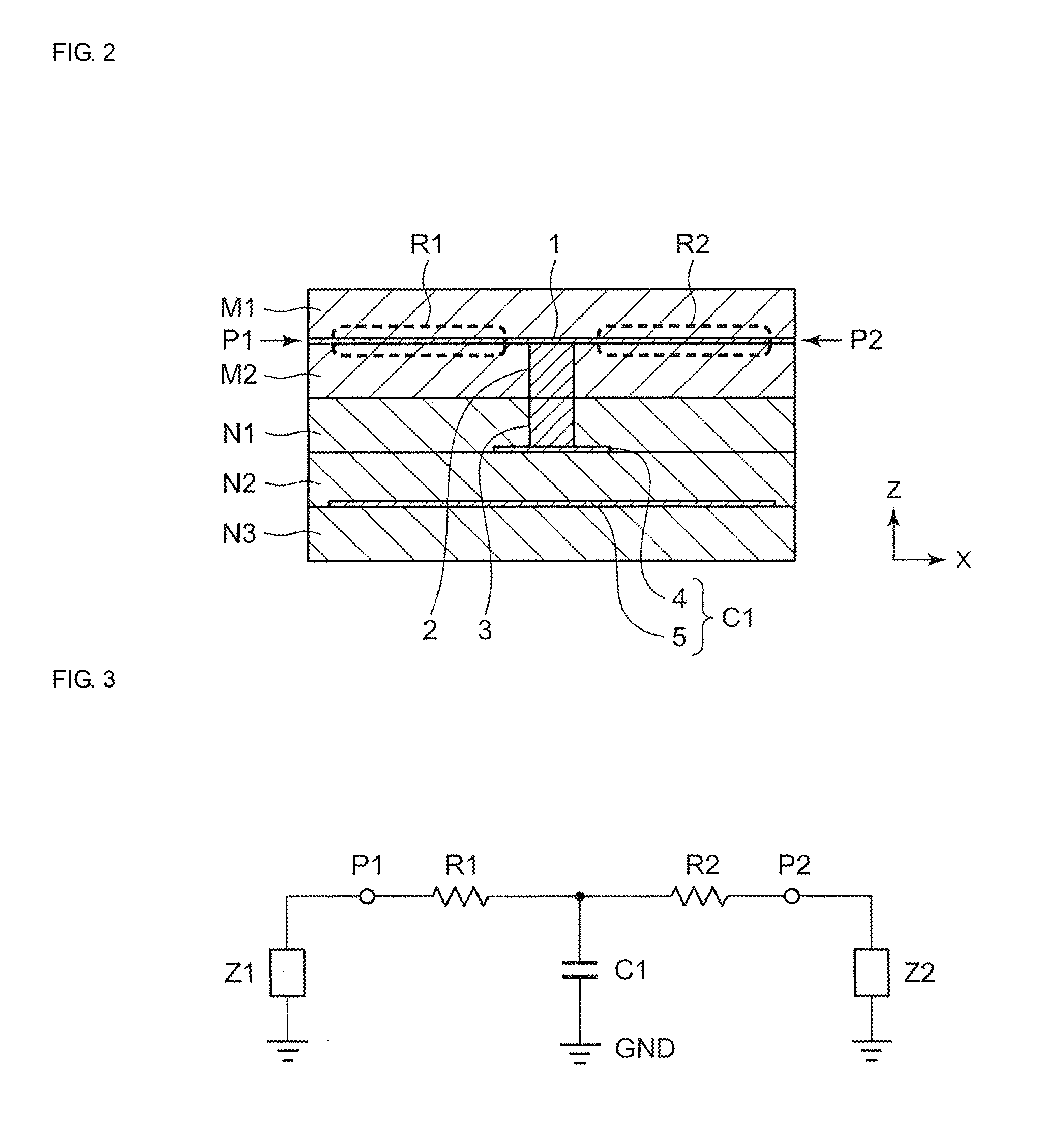
[0086]FIG. 1 is an exploded perspective view of the configuration of a high-frequency device according to a first embodiment of the present invention. FIG. 2 is a cross-sectional view of the high-frequency device illustrated in FIG. 1 in a multilayer stacked state. The cross-sectional view in FIG. 2 illustrates a cross section along a plane parallel to the XZ plane passing through the center of the high-frequency device in the Y-direction.
[0087]The high-frequency device illustrated in FIG. 1 is provided with a substrate including a plurality of layers stacked on top of one another, including at least one of dielectric layers N1 to N3 and at least one of magnetic layers M1 and M2. The high-frequency device includes at least one of pattern conductors 1, 4, and 5 each formed on one of the plurality of layers, and at least one of via conductors 2 and 3 each extending through one of the plurality of layers. A one-dot chain line between the magnetic layer M2 and the dielectric layer N1 an...
second embodiment
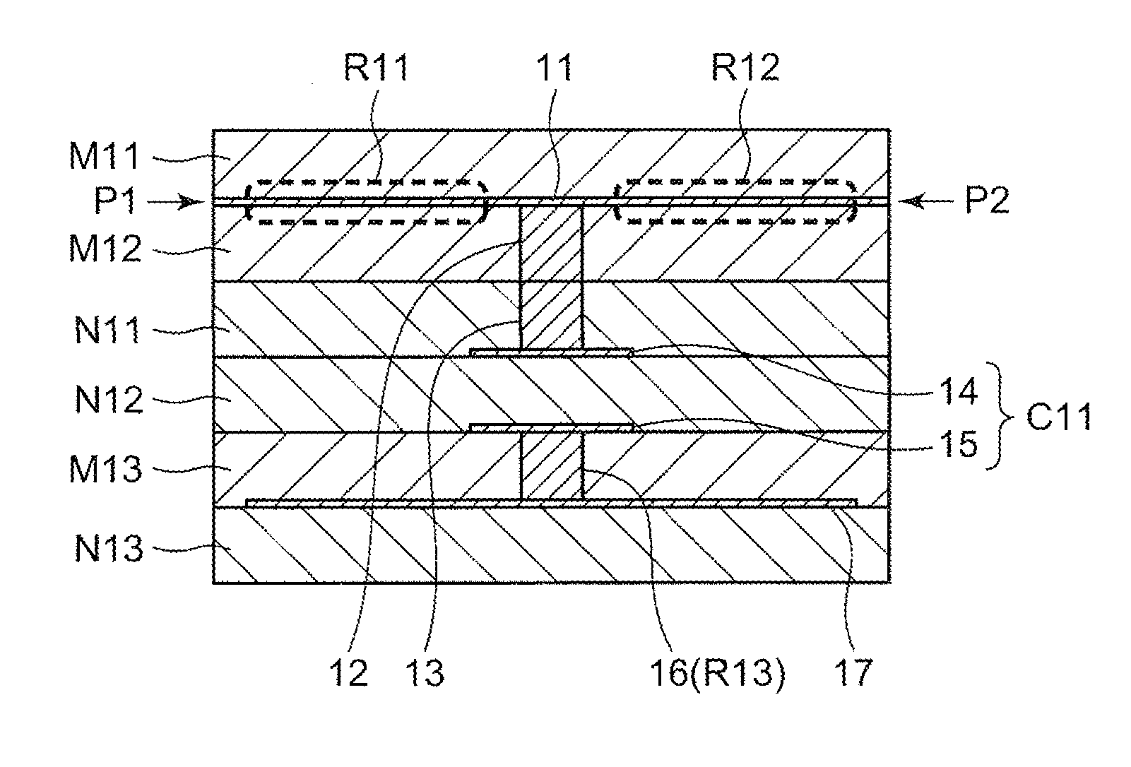
[0096]FIG. 5 is an exploded perspective view of the configuration of a high-frequency device according to a second embodiment of the present invention. FIG. 6 is a cross-sectional view of the high-frequency device illustrated in FIG. 5 in a multilayer stacked state.
[0097]The high-frequency device illustrated in FIG. 5 includes a substrate that includes a plurality of layers stacked on top of one another including dielectric layers N11 to N13 and magnetic layers M11 to M13. The high-frequency device includes pattern conductors 11, 14, 15, and 17 each formed on one of the plurality of layers and via conductors 12, 13, and 16 each extending through one of the plurality of layers. The high-frequency device further includes terminals P1 and P2 formed at the pattern conductor 11, and includes a ground terminal GND formed at the pattern conductor 17. The pattern conductors 11, 14, 15, and 17 and the via conductors 12, 13, and 16 connect the terminals P1 and P2 and the ground terminal GND t...
third embodiment
[0103]FIG. 9 is an exploded perspective view of the configuration of a high-frequency device according to a third embodiment of the present invention.
[0104]The high-frequency device illustrated in FIG. 9 includes a substrate that includes a plurality of layers stacked on top of one another including dielectric layers N21 to N23 and a magnetic layer M21. The high-frequency device includes pattern conductors 21 to 24 and 27 each formed on one of the plurality of layers, via conductors 25 and 26 each extending through one of the plurality of layers, and an inductor L21 including a pattern conductor formed on the at least one dielectric layer N21. The high-frequency device further includes terminals P1 and P2 and a ground terminal GND formed on each of the dielectric layers N21 to N23 and the magnetic layer M21. When the dielectric layers N21 to N23 and the magnetic layer M21 are stacked on top of one another, the terminals P1 and P2 and the ground terminal GND formed on one layer are r...
PUM
 Abstract
Description
Claims
Application Information