Optical element and method for producing the same

a technology of optical elements and optical elements, applied in the field of optical elements, can solve the problems of widening the absorbance spectrum and lowering the absorbance that can be obtained at the target wavelength, and achieve the effects of enhancing an electric field, reducing particle size variation, and easy production of optical elements

Inactive Publication Date: 2015-06-11
SEIKO EPSON CORP
View PDF4 Cites 1 Cited by
  • Summary
  • Abstract
  • Description
  • Claims
  • Application Information

AI Technical Summary

Benefits of technology

[0024]The method enables easily producing an optical element in which the metal particles on the substrate have controlled particle sizes and a reduced particle size variation, and that can desirably enhance an electric field by means of LSPR.

Problems solved by technology

However, a problem of the chips having an island structure is that the large size variation of the metal particles widens the absorbance spectrum, and lowers the absorbance that can be obtained at the target wavelength.

Method used


Image

  • Optical element and method for producing the same
  • Optical element and method for producing the same
  • Optical element and method for producing the same

Examples


Embodiment Construction

[0033]Some embodiments of the invention are described below. The following embodiments are intended to solely illustrate the invention. The invention is in no way limited by the following exemplary embodiments, and includes various modifications as may be appropriately made within the gist of the invention. It should also be noted that the configurations described below do not necessarily represent all the essential constituting elements of the invention.

1. OPTICAL ELEMENT PRODUCING METHOD

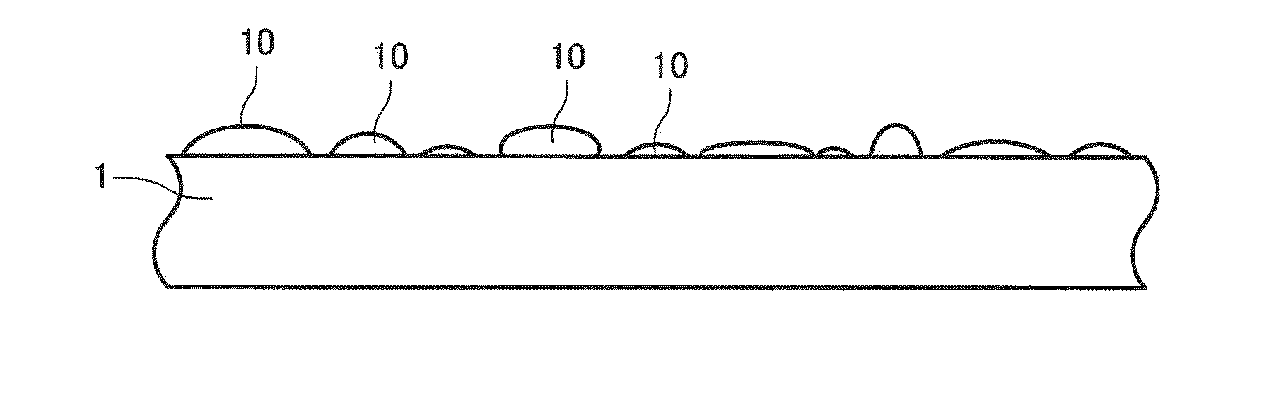
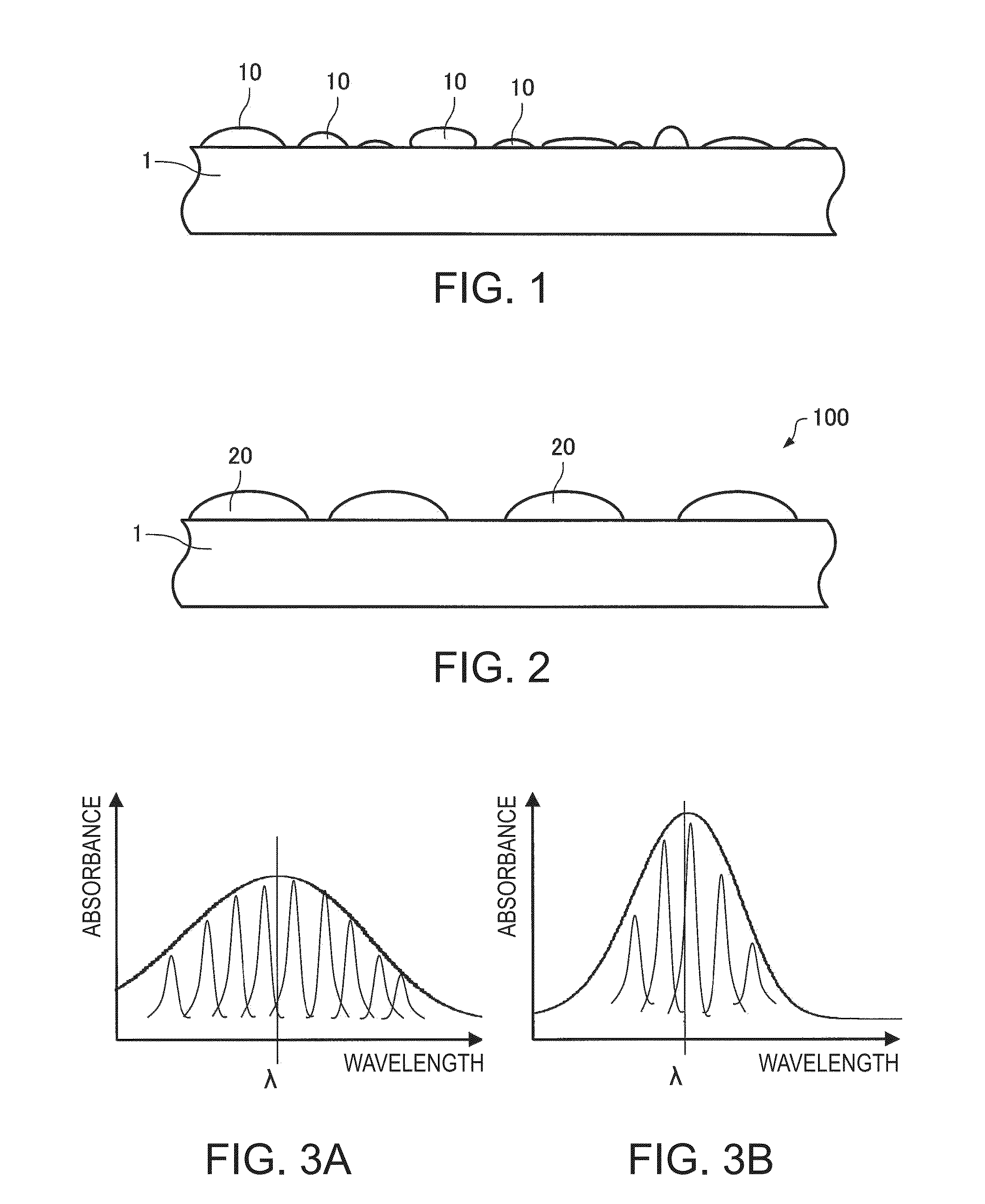
[0034]The optical element producing method of the present embodiment includes depositing a metal on a substrate in a particulate fashion, and heating the particulate metal in the presence of a compound that contains carbon and silicon. FIG. 1 is a cross sectional view schematically representing a state after a metal is deposited on a substrate 1 in a particulate fashion. FIG. 2 is a cross sectional view schematically representing a state after metal particles 20 are formed by the heating of a parti...


PUM

PropertyMeasurementUnit
particle sizeaaaaaaaaaa
temperatureaaaaaaaaaa

Abstract

An optical element is produced by depositing a metal on a substrate in a particulate fashion, and heating the particulate metal in the presence of a compound that contains carbon and silicon.

Description

BACKGROUND[0001]1. Technical Field[0002]The present invention relates to an optical element and a method for producing the same.[0003]2. Related Art[0004]In recent years, the demands for sensor chips used in applications such as medical diagnosis, and the testing of food and beverage have been increasing, and there is a need for the development of high-sensitive and small sensor chips. Sensor chips based on the electrochemical technique, and various other types of sensor chips have been studied to meet such demands. Sensor chips using surface plasmon resonance (SPR) spectroscopy, particularly surface enhanced Raman scattering have attracted interest because of advantages including integration, low cost, and the applicability to any measurement environment.[0005]Surface plasmons represent an oscillation mode of electron waves coupling to light under surface-inherent interface conditions. One method of exciting surface plasmons is to couple light to plasmons with a diffraction grating...

Claims


Application Information

Patent Timeline
Patent Type & Authority Applications(United States)
IPC IPC(8): G02B5/00G01N21/552
CPCG02B5/008G01N2201/06113G01N21/554B82Y20/00B82Y40/00G01N21/658
Inventor YAMADA, AKIKOYAMADA, KOHEI
Owner SEIKO EPSON CORP
Why Eureka
Try Eureka