Method and device for testing semiconductor subtrates for radiofrequency application

a technology of radiofrequency applications and semiconductor substrates, applied in resistance/reactance/impedence, voltage-current phase angle, instruments, etc., can solve problems such as transmission loss or “insertion loss, parasitic signals that are particularly disadvantageous for radiofrequency applications

Inactive Publication Date: 2015-06-18
SOITEC SA
View PDF4 Cites 21 Cited by
  • Summary
  • Abstract
  • Description
  • Claims
  • Application Information

AI Technical Summary

Benefits of technology

[0038]More precisely, the lower this criterion is, the better the RF performance of devices fabricated on the substrate.

Problems solved by technology

Because at high frequencies electric fields penetrate into the substrate and affect any charge carriers that they encounter, substrates for radiofrequency devices are subject to, on the one hand, transmission loss or “insertion loss,” or, on the other hand, behavior-modifying crosstalk between devices through the substrate.
These harmonic waves and their combinations may generate parasitic signals that are particularly disadvantageous for radiofrequency applications.
Verifying that a substrate is suitable for radiofrequency applications is, therefore, a problem.
However, producing and then taking measurements using these test structures is a long and costly process.
Furthermore, the facilities needed to measure RF performance are expensive and substrate manufacturers normally do not have such facilities at their disposal.
Substrate manufacturers are, therefore, not themselves able to test the qualification, with respect to RF performance, of the substrates that they supply.
However, this method gives only an incomplete indication of the resistivity of the substrate because the electrodes are merely applied to the surface of the substrate and, therefore, only allow the average resistivity of the substrate to be measured.
However, even though substrate manufacturers are able to guarantee that the substrates that they supply meet particular specifications in terms of electrical resistivity, these specifications are uncorrelated with the RF performance of the devices that will subsequently be fabricated on these substrates.

Method used


Image

  • Method and device for testing semiconductor subtrates for radiofrequency application
  • Method and device for testing semiconductor subtrates for radiofrequency application
  • Method and device for testing semiconductor subtrates for radiofrequency application

Examples


Embodiment Construction

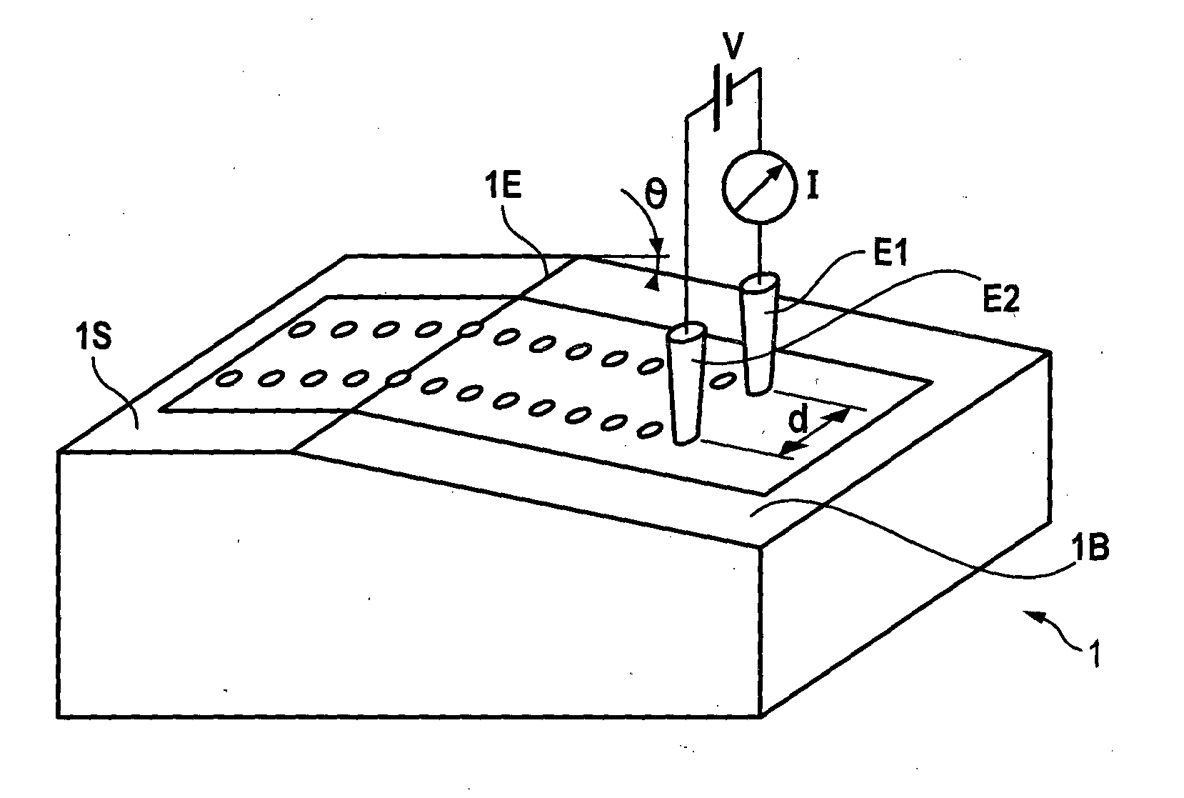
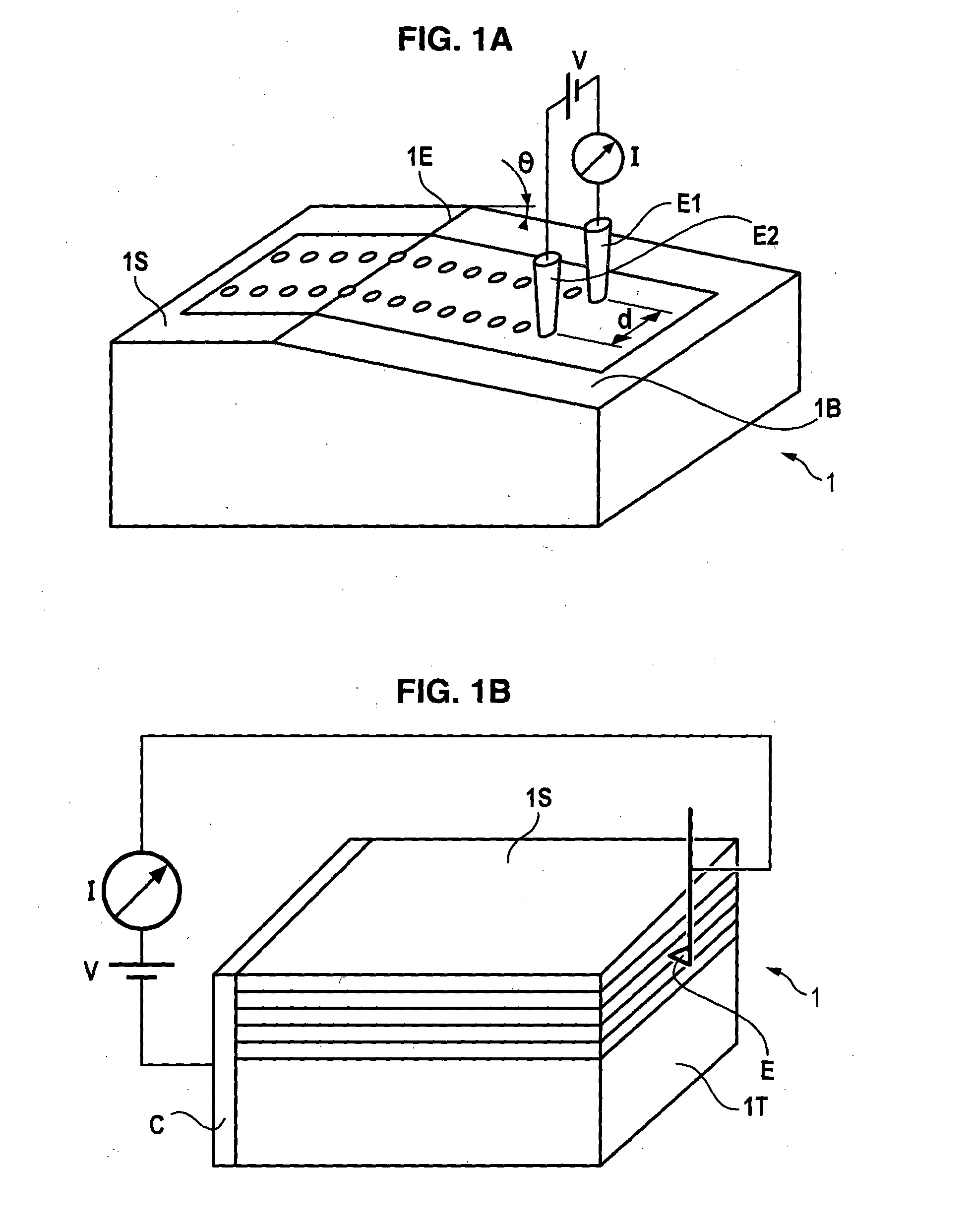
[0054]The resistivity profile of the substrate may be determined using any appropriate method.

[0055]Preferably, the spreading resistance profiling (SRP) method is used, the implementation of which is illustrated in FIG. 1A.

[0056]With reference to FIG. 1A, the SRP method is implemented on a semiconductor substrate 1 that has already been polished, from its flat top side 1S (on which the radiofrequency devices are intended to be formed), so as to produce a chamfer 1B extending from an edge stop 1E on the side 1S, the chamfer 1B having an angle θ that allows the desired depth in the substrate 1 to be reached.

[0057]The substrate may be made of any semiconductor material suitable for radiofrequency applications.

[0058]Among preferred materials, mention may be made of high-resistivity (HR) silicon (i.e., having an electrical resistivity higher than 500 ohm·cm, preferably higher than 1000 ohm·cm, and even higher than 3000 ohm·cm).

[0059]The substrate may optionally be a semiconductor-on-insu...


PUM

PropertyMeasurementUnit
electrical resistivityaaaaaaaaaa

Abstract

The invention relates to a method for testing a semiconductor substrate (1) for radiofrequency applications, characterized in that the electrical resistivity profile of the substrate as a function of depth, is measured and, using the profile, a criterion is calculated, defined by the formula (I): where D is the integration depth, σ(x) is the electrical conductivity measured at a depth x in the substrate, and L is a characteristic attenuation length of the electric field in the substrate. The invention also relates to a method for selecting a semiconductor substrate (1) for radiofrequency applications and to a device for implementing these methods.

Description

CROSS-REFERENCE TO RELATED APPLICATIONS[0001]This application is a national phase entry under 35 U.S.C. §371 of International Patent Application PCT / IB2013 / 000044, filed Jan. 15, 2013, designating the United States of America and published in English as International Patent Publication WO 2013 / 108107 A1 on Jul. 25, 2013, which claims the benefit under Article 8 of the Patent Cooperation Treaty and under 35 U.S.C. §119(e) to French Patent Application Serial No. 1250396, filed Jan. 16, 2012, the disclosure of each of which is hereby incorporated herein in its entirety by this reference.TECHNICAL FIELD[0002]The present invention relates to a method and device for testing a semiconductor substrate for radiofrequency applications, and to a method and device for selecting semiconductor substrates for such applications.BACKGROUND[0003]Semiconductor substrates used to form radiofrequency (RF) devices must have a high electrical resistivity, i.e., typically higher than 500 ohm·cm, preferably...

Claims


Application Information

Patent Timeline
Patent Type & Authority Applications(United States)
IPC IPC(8): G01N27/04
CPCG01N27/041G01R31/2831
Inventor ALLIBERT, FREDERIC
Owner SOITEC SA
Why Eureka
Try Eureka