Optical waveguide, optical interconnection component, optical module, opto-electric hybrid board, and electronic device

a technology of optical interconnection and optical module, applied in the direction of optical waveguide light guide, optical light guide, instrument, etc., can solve the problems of increased transmission loss, difficult coexistence of electrical elements and optical elements in planar view, etc., and achieve high density mounting of electrical wiring and optical wiring, easy assembly and repair, and high performance

Inactive Publication Date: 2015-06-18
SUMITOMO BAKELITE CO LTD
View PDF22 Cites 38 Cited by
  • Summary
  • Abstract
  • Description
  • Claims
  • Application Information

AI Technical Summary

Benefits of technology

[0080]In accordance with the present invention, an opto-electric hybrid board in which optical wiring is freely disposed without restriction by the arrangement of electrical elements and the like, and in which high-density mounting of electrical wiring and optical wiring is possible can be obtained.
[0081]Also, since detachment of an optical waveguide in which optical wiring has been constructed is possible, on opto-electric hybrid board for which assembly and repair are easy can be obtained.
[0082]Also, in accordance with the present invention, an electrical device comprising the above-mentioned opto-electric hybrid, and for which miniaturization and high performance has been made possible, can be obtained.
[0083]Furthermore, in accordance with the present invention, an optical waveguide which, when mounted so as be superimposed on the electrical wiring board, has made possible the free construction of optical wiring while retaining heat dissipation of electrical elements disposed on the electrical wiring board can be obtained.
[0084]Also, in accordance with the present invention, an optical interconnection component, an optical module, an opto-electric hybrid board, and an electronic device including high-density optical wiring can be obtained.

Problems solved by technology

However, since it is necessary for these electrical elements to be fixed to the substrate by solder or the like, it is difficult for the electrical elements and the optical elements to coexist in the same position in planar view.
As a result, the higher the mounting density of electrical elements becomes, the more many optical waveguides must be intricately disposed, and the number of production steps becomes very large and the total extension of the optical waveguide increases, thus leading to increase in transmission loss.

Method used


Image

  • Optical waveguide, optical interconnection component, optical module, opto-electric hybrid board, and electronic device
  • Optical waveguide, optical interconnection component, optical module, opto-electric hybrid board, and electronic device
  • Optical waveguide, optical interconnection component, optical module, opto-electric hybrid board, and electronic device

Examples


first embodiment

[0119]Firstly, a first embodiment of the opto-electric hybrid board of the present invention is explained.

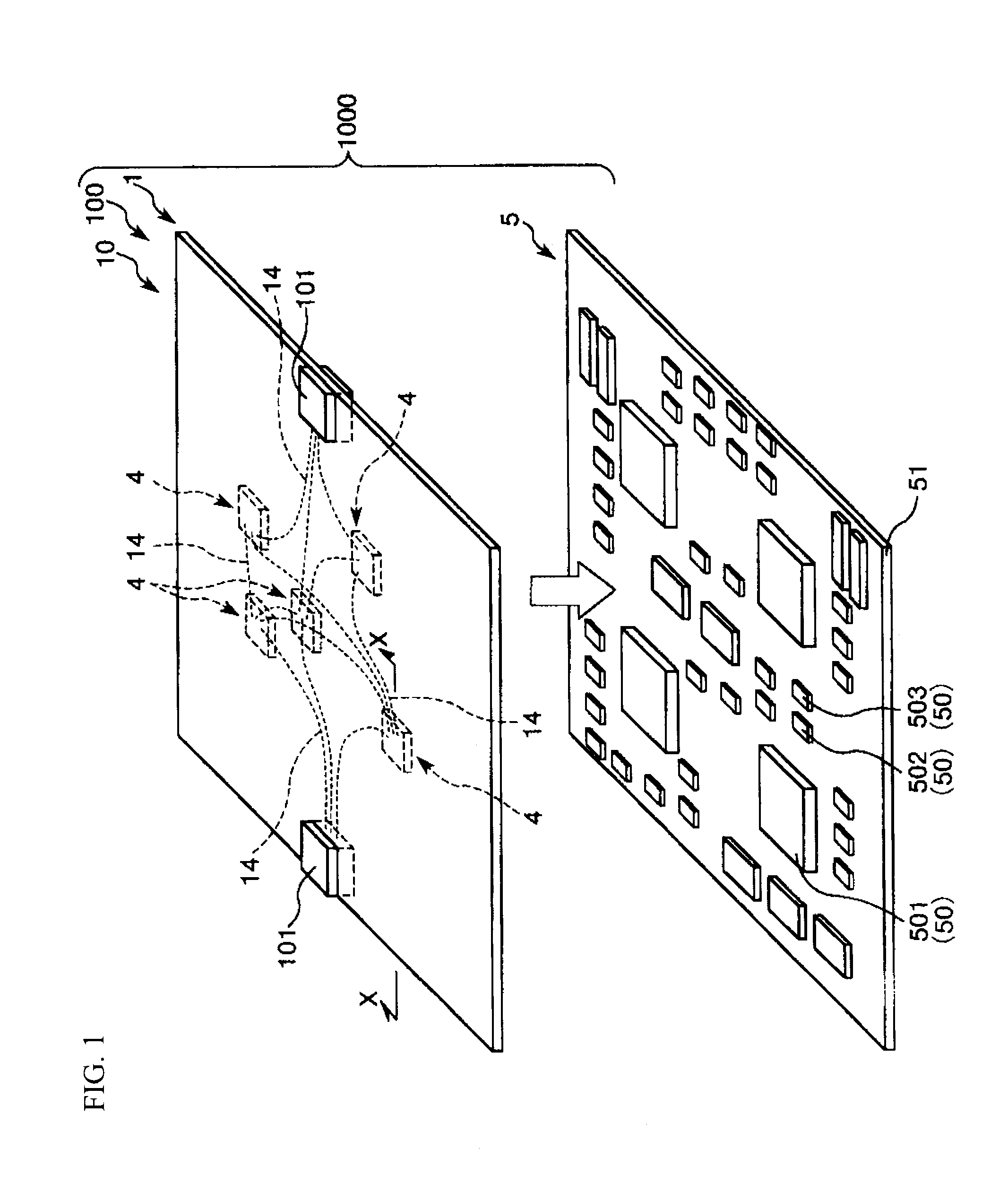
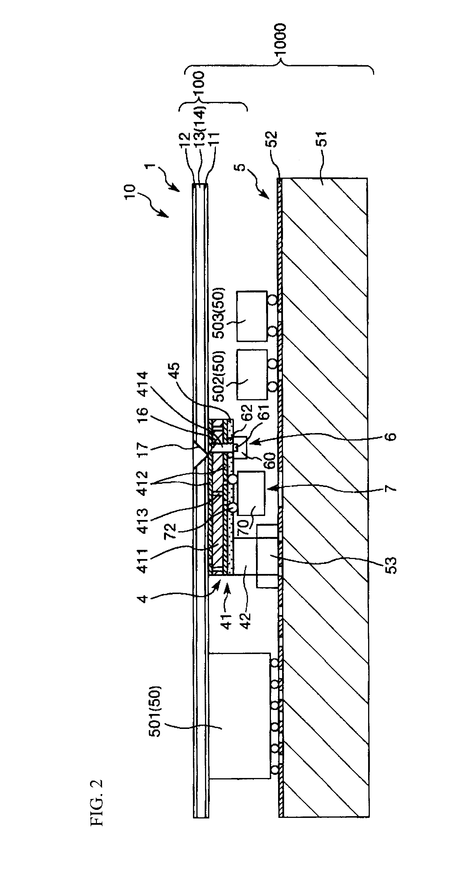
[0120]FIG. 1 is a perspective view (shown partially cutaway and see-through) showing the first embodiment of the opto-electric hybrid board of the present invention and FIG. 2 is a line X-X cross-sectional view in the state in which the optical waveguide is superimposed as shown by the void arrow in FIG. 1.

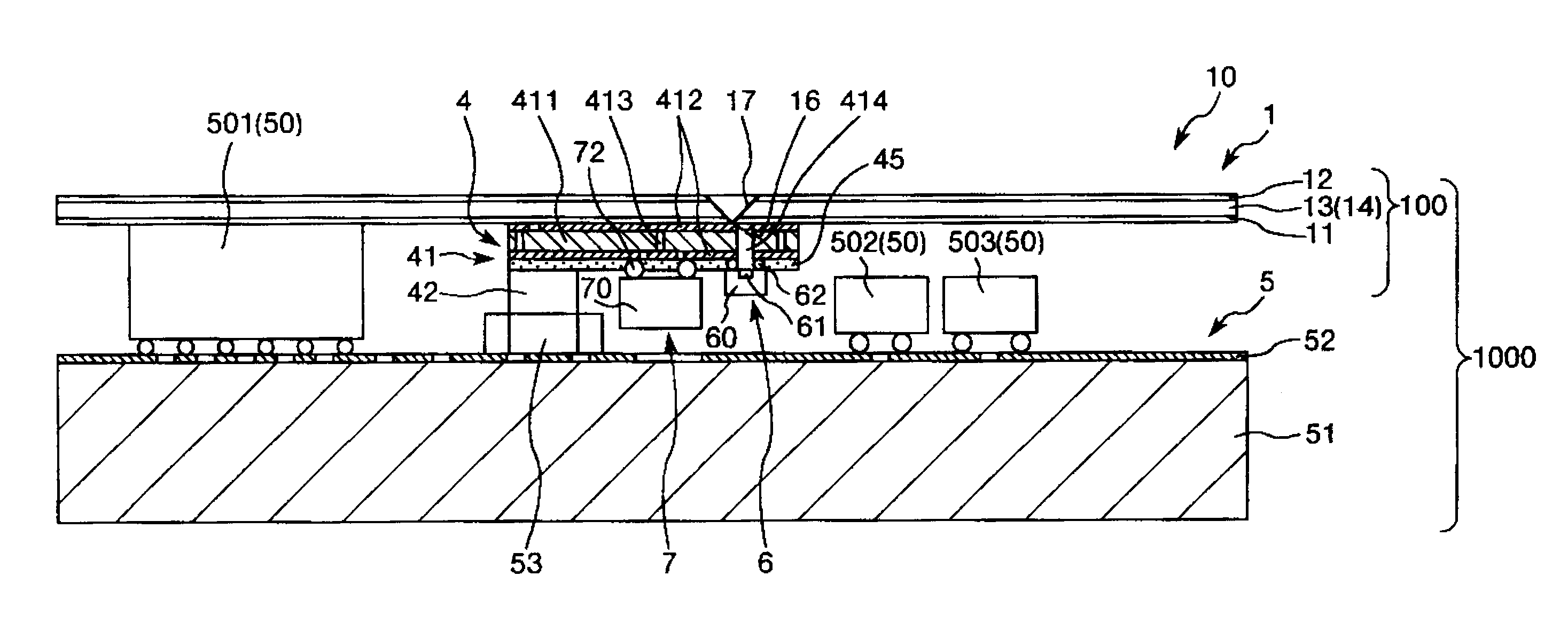
[0121]An optical module 100 shown in FIG. 1 has an optical waveguide 1, an optical connector 101 disposed at an end section thereof, and an opto-electric conversion section 4 disposed below the optical waveguide 1. Also, an opto-electric hybrid board 1000 shown in FIG. 1 has the optical module 100, and a motherboard (electrical wiring board) 5 disposed below the opto-electric conversion section 4.

[0122]Of these, the optical waveguide 1 is a sheet-like member forming a quadrangle in the planar view. The optical waveguide 1, as shown in FIG. 2, is formed by stacking a cladding l...

second embodiment

[0273]Next, the optical module according to a second embodiment of the opto-electric hybrid board of the present invention is explained.

[0274]FIG. 13 is a cross-sectional view showing a part of the second embodiment of the opto-electric hybrid board of the present invention.

[0275]Hereinafter, although the second embodiment is explained, it is explained by placing emphasis on the points of difference with the first embodiment, and an explanation of the same matters is omitted. Also, in FIG. 13, the same constitutional parts as the first embodiment are labeled with the same reference numerals as those previously explained and a detailed explanation thereof is omitted.

[0276]Other than the constitution of the opto-electric conversion section 4 being different, the second embodiment is the same as the first embodiment.

[0277]The opto-electric conversion section 4 shown in FIG. 13 has an insulating substrate 411a disposed on the lower surface of the cladding layer 11 of the optical wavegui...

third embodiment

[0282]Next, a third embodiment of the opto-electric hybrid board of the present invention is explained.

[0283]FIG. 14 is a cross-sectional view showing a part of the third embodiment of the opto-electric hybrid board of the present invention.

[0284]Hereinafter, although the third embodiment is explained, it is explained by placing emphasis on the points of difference with the first embodiment, and an explanation of the same matters is omitted. Also, in FIG. 14, the same constitutional components as each of the above-mentioned embodiments are labeled with the same reference numerals as those previously explained and a detailed explanation thereof is omitted.

[0285]Other than having an electrical interposer (electrical wiring board) 55 interposed between the opto-electric conversion section 4 and the motherboard 5, and the LSI 501 mounted on the electrical interposer 55, the third embodiment is the same as the first embodiment. In addition, different to the first and second embodiments, ...


PUM


Abstract

In accordance with the present invention, an opto-electric hybrid board in which optical wiring is freely disposed without restriction by the arrangement of electrical elements and the like, and in which high-density mounting of electrical wiring and optical wiring is possible, and an electric device including this opto-electric hybrid board are provided. An opto-electrical hybrid board (1000) of the present invention has an optical waveguide (1), an optical connector disposed at an end section of the optical waveguide (1), and an opto-electric conversion section (4) disposed below the optical waveguide (1), and a motherboard (electrical wiring board) (5) disposed below the opto-electric conversion portion (4). Of these, the optical waveguide (1) includes a core layer (13) including a plurality of core sections (14) being configured to intersect with each other at one plane and side surface cladding sections, and a mirror (optical path conversion section) 17 converting the optical path of the core sections (14). Also, between the optical waveguide (1) and the motherboard (5) is connected via an electrical connector and preferably both the optical waveguide (1) and the motherboard (5) are detachable.

Description

TECHNICAL FIELD[0001]The present application relates to an optical waveguide, an optical interconnection component, an optical module, an opto-electric hybrid board, and an electronic device.[0002]The present application claims priority on Japanese Patent Application No. 2012-138118, filed Jun. 19, 2012, Japanese Patent Application No. 2012-138119, filed on Jun. 19, 2012, Japanese Patent Application No. 2012-138120, filed Jun. 19, 2012, Japanese Patent Application No. 2013-125972, filed Jun. 14, 2013, and Japanese Patent Application No. 2013-125973, filed Jun. 14, 2013, the content of which are incorporated herein by reference.BACKGROUND ART[0003]Optical communication technology transferring data using optical carrier waves has been developed, and an optical waveguide has become widespread as a means for leading such optical carrier waves from one point to another point. This optical waveguide has a linear core section and a cladding section provided so as to cover the periphery the...

Claims


Application Information

Patent Timeline
Patent Type & Authority Applications(United States)
IPC IPC(8): G02B6/122G02B6/42
CPCG02B6/122G02B6/4274G02B6/4257G02B6/125G02B6/428G02B6/43
Inventor ARAI, SHINYA
Owner SUMITOMO BAKELITE CO LTD
Why Eureka
Try Eureka