Semiconductor device

a semiconductor and gate technology, applied in the direction of semiconductor devices, basic electric elements, electrical equipment, etc., can solve problems such as still exist, and achieve the effect of reducing remarkably the electric field applied

Active Publication Date: 2015-06-18
TOYOTA JIDOSHA KK +1
View PDF8 Cites 13 Cited by
  • Summary
  • Abstract
  • Description
  • Claims
  • Application Information

AI Technical Summary

Benefits of technology

[0009]In the semiconductor device, in the off-state, from the pn junction location of the second semiconductor region and the drift layer, a depletion layer extends. Under such conditions, the second semiconductor region is electrically conductive with the first main electrode or the body layer and becomes the same potential as the first main electrode or the body layer. Therefore, compared with a case in which the second semiconductor region is the floating region, the depletion layer can be extended from the pn junction location, which makes it possible to reduce remarkably the electric field applied to the gate oxide film.

Problems solved by technology

Also in the semiconductor device according to JP 2005-116822 A, this problem still exists.

Method used


Image

  • Semiconductor device
  • Semiconductor device
  • Semiconductor device

Examples


first embodiment

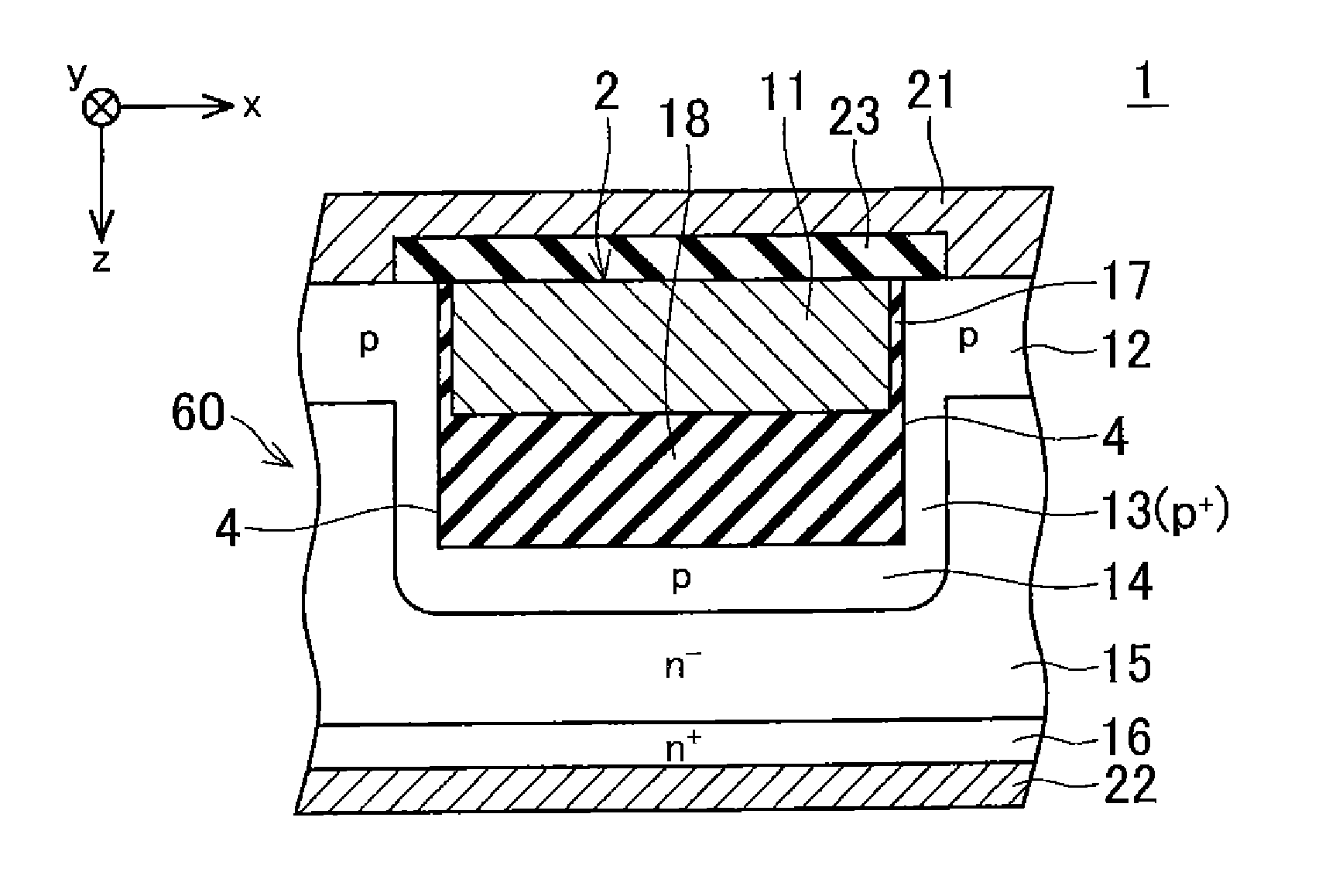
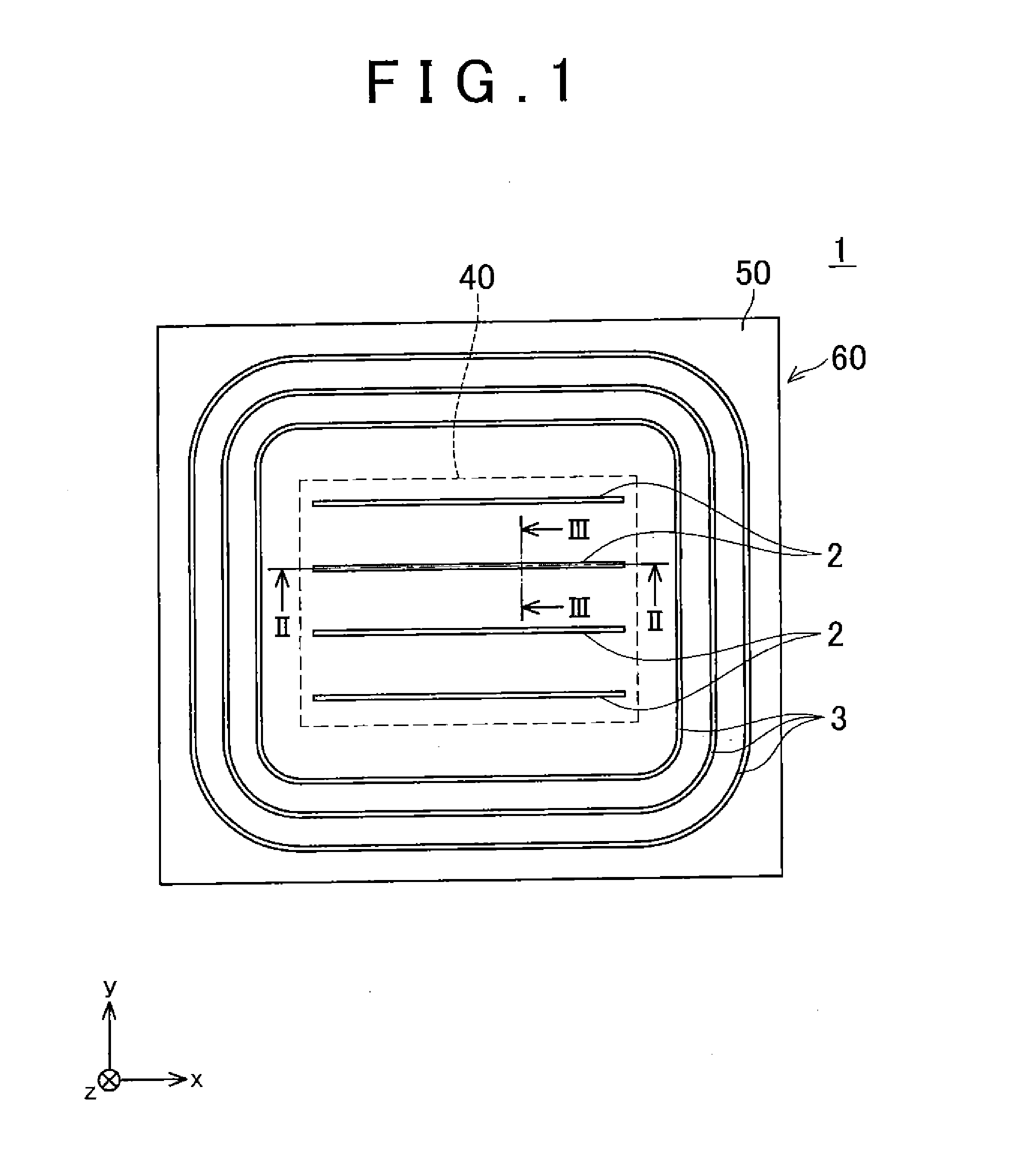
[0031]Hereinafter, with reference to drawings, a semiconductor device of the present invention will be described. As shown in FIG. 1, a semiconductor device 1 of the present embodiment includes a semiconductor substrate 60, electrodes, an insulation film and other elements. The electrodes, insulation film and other elements are formed on an upper surface and a lower surface of the semiconductor substrate 60 and not shown in FIG. 1. The semiconductor substrate 60 is a SiC substrate and includes a cell area 40 in which a current flows and a terminal area 50 that surrounds the cell area 40. In the cell area 40, a plurality of gate trenches 2 are disposed. The plural gate trenches 2 extend linearly in an X-direction and disposed spaced apart in a Y-direction. In the terminal area 50, a plurality of terminal trenches 3 are disposed. The terminal trench 3 is formed annularly so as to surround the cell area 40. A corner part of the terminal trench 3 is formed into an arc shape. In the pres...

second embodiment

[0055]Other than the manufacturing method shown in FIGS. 8 to 11, another method which is shown in FIGS. 12 to 15 is available for manufacturing the semiconductor device 1a of the That is, as shown in FIG. 12, firstly, a gate trench 2a is formed in the semiconductor substrate 60, and the diffusion region 14 is formed in a bottom part of the gate trench 2a. The gate trench 2a and the diffusion region 14 are formed in the same manner as the conventional method.

[0056]Next, as shown in FIG. 13, silicon oxide 48 is filled in the gate trench 2a by a CVD method. Then, as shown in FIG. 14, a part of the silicon oxide 48 filled in the gate trench 2a is removed by etching, and a trench 52 for forming the gate electrode 11a is formed. Next, as shown in FIG. 15, a part of the silicon oxide 48 is removed by further etching, and a trench 54 for forming the conductor region 30 is formed thereby. When the trenches 52 and 54 are formed, the poly-silicon is filled in the trenches 52 and 54 according...


PUM


Abstract

A semiconductor device includes: a drift layer having a first conductivity type; a body layer having a second conductivity type; a first semiconductor region having the first conductivity type; a gate insulation film; a trench gate electrode; a first main electrode; a second semiconductor region having the second conductivity type; and a conductor region. The first main electrode is electrically connected with the body layer and the first semiconductor region. The second semiconductor region is disposed on a bottom part of the gate trench, and is surrounded by the drift layer. The conductor region is configured to electrically connect the first main electrode with the second semiconductor region and is configured to equalize, when the semiconductor device is in an off-state, a potential of the second semiconductor region and a potential of the first main electrode.

Description

INCORPORATION BY REFERENCE[0001]The disclosure of Japanese Patent Application No. 2013-259764 filed on Dec. 17, 2013 including the specification, drawings and abstract is incorporated herein by reference in its entirety.BACKGROUND OF THE INVENTION[0002]1. Field of the Invention[0003]The present invention relates to a trench gate semiconductor device. In more detail, the present invention relates to a technology that alleviates an electric field applied to a gate oxide film that covers a trench gate electrode.[0004]2. Description of Related Art[0005]Japanese Patent Application Publication No. 2005-116822 (JP 2005-116822 A) discloses a trench gate semiconductor device (power MOS) that controls electric continuity between a drain and a source by voltage application to a gate electrode. The semiconductor device includes a gate trench that penetrates through a body layer from an upper surface of a semiconductor substrate and extends to an inside of a drift layer. A floating region is for...

Claims


Application Information

Patent Timeline
Patent Type & Authority Applications(United States)
IPC IPC(8): H01L29/423H01L29/78
CPCH01L29/4236H01L29/7813H01L29/42368H01L29/66734H01L29/0623H01L29/1095
Inventor TAKAYA, HIDEFUMIWATANABE, YUKIHIKOAOI, SACHIKOAKIBA, ATSUYA
Owner TOYOTA JIDOSHA KK
Why Eureka
Try Eureka