Organic light emitting display device and method of manufacturing the same

a light-emitting display and organic technology, applied in the direction of solid-state devices, transistors, thermoelectric devices, etc., can solve the problems of high power consumption of passive matrix organic light-emitting display devices, limited resolution, and limited brightness, so as to increase the capacitance of storage capacitors, reduce the number of masks used, and increase manufacturing efficiency

Active Publication Date: 2015-07-02
LG DISPLAY CO LTD
View PDF2 Cites 26 Cited by
  • Summary
  • Abstract
  • Description
  • Claims
  • Application Information

AI Technical Summary

Benefits of technology

[0023]Another aspect of the present invention provides a method of manufacturing an organic light emitting display device, which decreases the number of masks used in a process of manufacturing a TFT, thereby increasing the manufacturing efficiency.
[0024]Another aspect of the present invention provides an organic light emitting display device and a method of manufacturing the same, which can increase a capacitance of a storage capacitor.

Problems solved by technology

Liquid crystal display (LCD) devices, which are widely used, need a backlight as a light source, and have technical limitations in brightness, contrast, and a viewing angle.
For this reason, the passive matrix organic light emitting display devices have high power consumption, and are limited in resolution.
Moreover, a kickback increases, and the boosting efficiency is reduced, causing a problem of an image quality of an OLED panel.
For this reason, it is difficult to apply a high-resolution OLED panel.
However, since an oxide TFT has vulnerable characteristic in which a characteristic of a device is changed by light, a light shield should be separately formed under the active layer 30.
As such, the process time and cost increase.

Method used


Image

  • Organic light emitting display device and method of manufacturing the same
  • Organic light emitting display device and method of manufacturing the same
  • Organic light emitting display device and method of manufacturing the same

Examples


first embodiment

[0100]FIGS. 9 and 10 are views illustrating a method of manufacturing a switching TFT according to the present invention. FIGS. 9 and 10 illustrate the method of manufacturing the switching TFT included in a pixel circuit unit. The switching TFT is formed in an ESL type.

[0101]The method of manufacturing an organic light emitting display device according to the first embodiment of the present invention forms the source, drain, and lower gate of the switching TFT on the same layer, and forms the lower gate as a light shield.

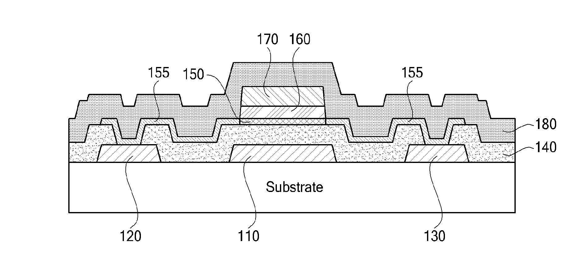
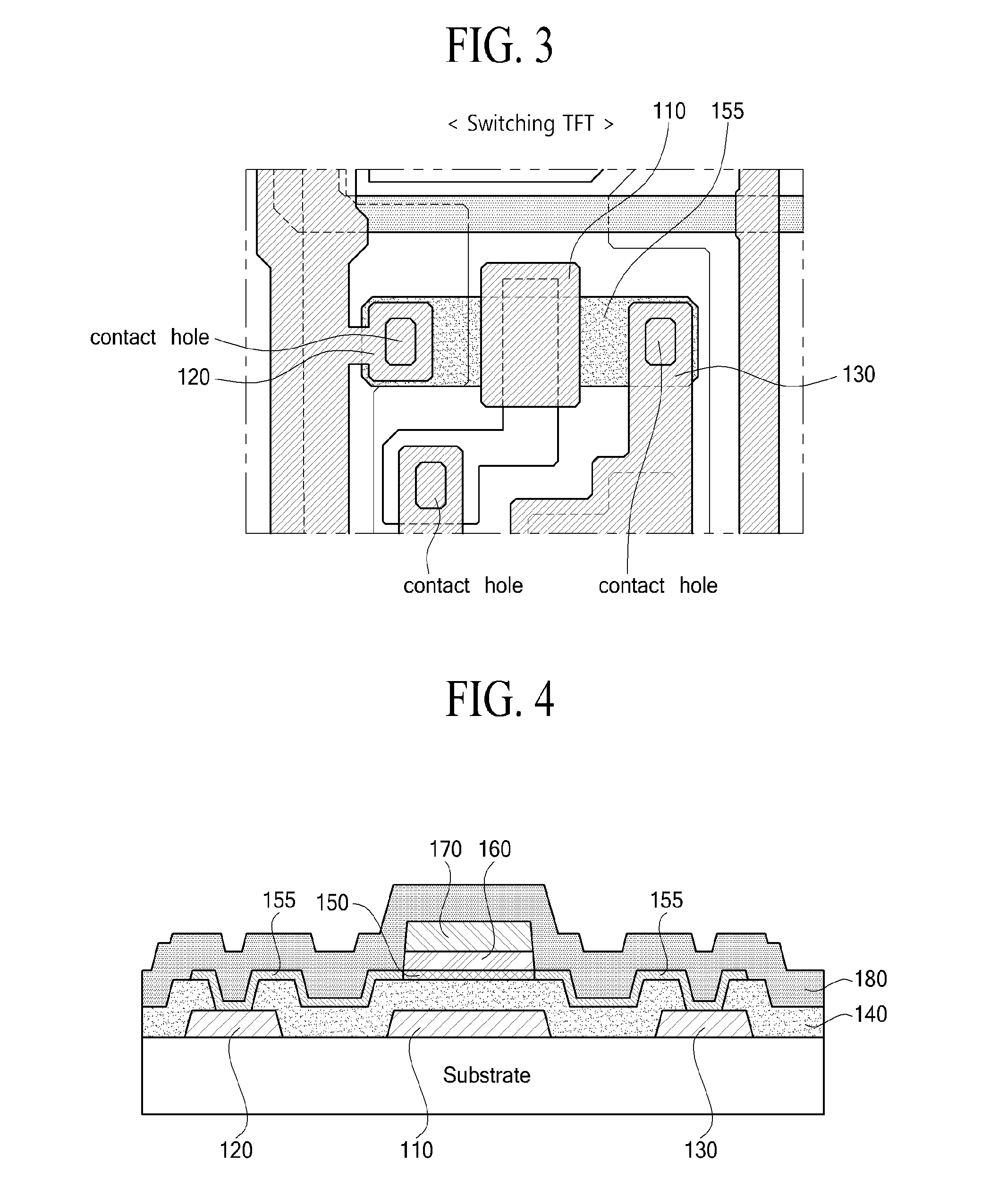
[0102]Referring to FIG. 9A, a conductive metal material is coated on a substrate, and then, by performing a first mask process, the lower gate 110, the source 120, and the drain 130 are formed in the switching TFT (SW-TFT) area.

[0103]The lower gate 110, the source 120, and the drain 130 are formed of the same metal on the same layer. Here, the lower gate 110 may perform a function of a light shield, in addition to a function of a gate of a TFT.

[0104]The lower gate ...

second embodiment

[0122]FIGS. 11 and 12 are views illustrating a method of manufacturing a switching TFT according to the present invention. FIGS. 11 and 12 illustrate the method of manufacturing the switching TFT included in the pixel circuit unit. The switching TFT is formed in an ESL type.

[0123]According to the first embodiment described above with reference to FIGS. 9 and 10, the switching TFT may be formed by performing the sixth mask process. According to the second embodiment to be described below with reference to FIGS. 11 and 12, the switching TFT may be formed by performing the fifth mask process.

[0124]The method of manufacturing an organic light emitting display device according to the second embodiment of the present invention forms the source, drain, and lower gate of the switching TFT on the same layer, and forms the lower gate as a light shield.

[0125]Referring to FIG. 11A, a conductive metal material is coated on a substrate, and then, by performing a first mask process, the lower gate...


PUM


Abstract

Disclosed is an organic light emitting display device. The organic light emitting display device includes a switching thin film transistor (TFT) that includes a lower gate, a source, and a drain formed on a substrate and on the same layer, a first gate insulating layer formed to cover the lower gate, the source, and the drain, an active layer formed on the first gate insulating layer, a conductive line formed to contact the source and the drain, a second gate insulating layer formed on the active layer, and an upper gate formed on the second gate insulating layer. The lower gate of the switching TFT is a light shield that blocks light from being irradiated onto the active layer.

Description

CROSS-REFERENCE TO RELATED APPLICATIONS[0001]This application claims the benefit of the Korean Patent Application No. 10-2013-0169457 filed on Dec. 31, 2013, which is hereby incorporated by reference for all purposes as if fully set forth herein.BACKGROUND OF THE INVENTION[0002]1. Field of the Invention[0003]The present invention relates to an organic light emitting display device. More particularly, the present invention relates to an organic light emitting display device that blocks light from being irradiated onto an oxide thin film transistor (TFT) by using a light shield formed of a source / drain metal, and a method of manufacturing the same which can reduce the number of masks to increase manufacturing efficiency.[0004]2. Discussion of the Related Art[0005]Liquid crystal display (LCD) devices, which are widely used, need a backlight as a light source, and have technical limitations in brightness, contrast, and a viewing angle. Organic light emitting devices, on the other hand, ...

Claims


Application Information

Patent Timeline
Patent Type & Authority Applications(United States)
IPC IPC(8): H01L27/32H01L29/788H01L29/786
CPCH01L27/3276H01L27/3272H01L29/7869H01L29/788H01L29/78648H01L29/78633H01L29/786H10K59/00H10K59/126H10K59/131H10K59/1213
Inventor SEO, HYUN SIKSHIM, JONG SIKSEO, KYUNG HANCHOI, YONG HOPARK, HYO JIN
Owner LG DISPLAY CO LTD
Why Eureka
Try Eureka