

Method for manufacturing semiconductor device
a manufacturing method and semiconductor technology, applied in the direction of semiconductor devices, electrical devices, transistors, etc., can solve the problems of large distance between the contact area (or contact aperture, ca) and the gate spacer, and the enhancement of the properties of small devices is severely restricted, so as to reduce the parasitic resistance of the device, reduce the spacing, and increase the contact area
- Summary
- Abstract
- Description
- Claims
- Application Information
AI Technical Summary
Benefits of technology
Problems solved by technology
Method used
Image

Examples
Embodiment Construction
[0020]The characteristics and technical effects of the technical solution of the present invention is described in detail referring to the figures in combination with schematic embodiments. What should be noted is that: similar reference signs denote similar structures, and the terms “first”, “second”, “above”, “below”, “thick”, “thin”, and so on used in the present application can be used for modifying various device structures. These modifications, unless otherwise stated, do not imply the space, order, or hierarchical relationship of the device structure modified.
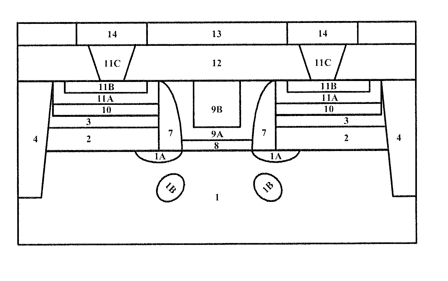
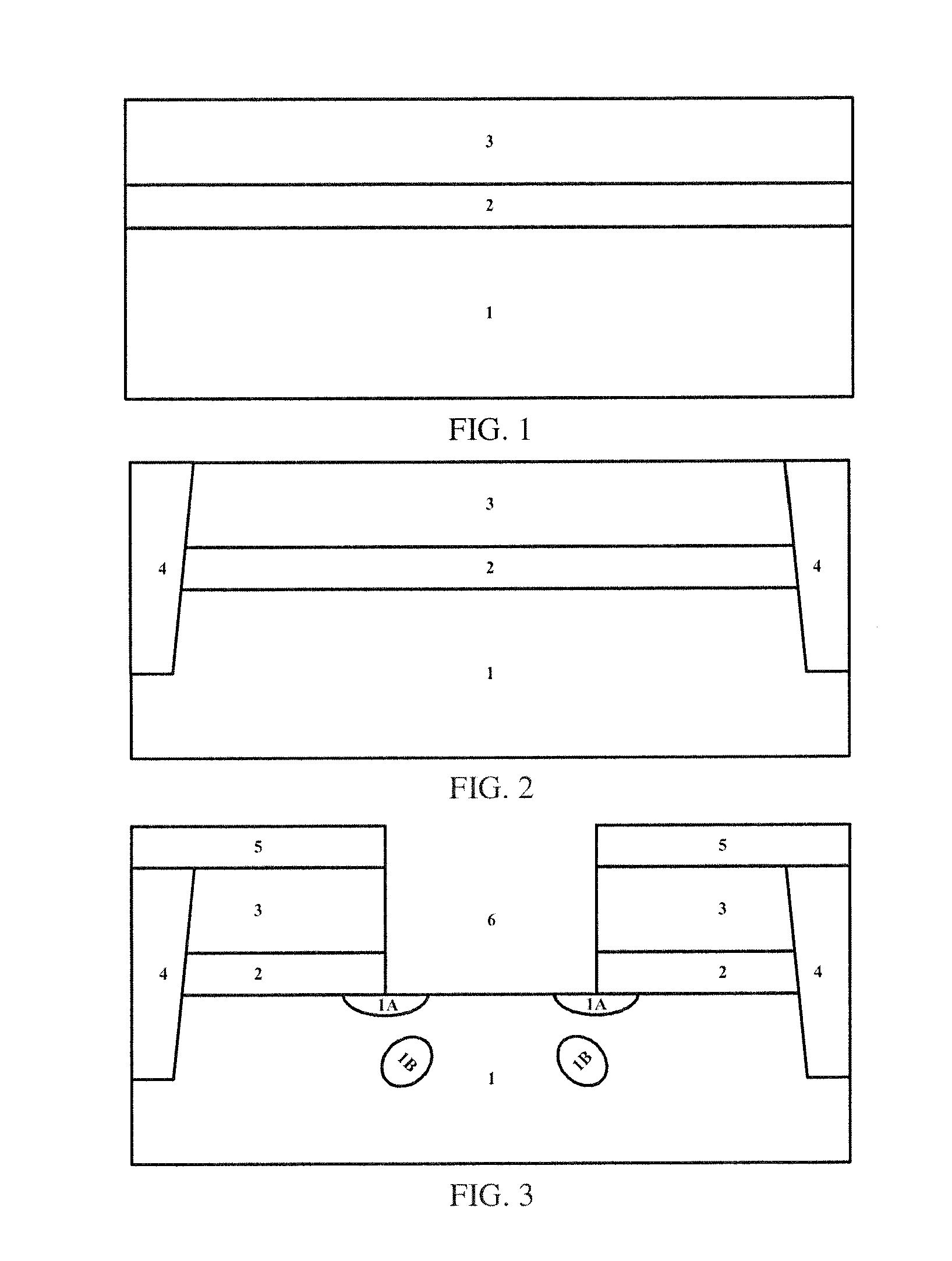
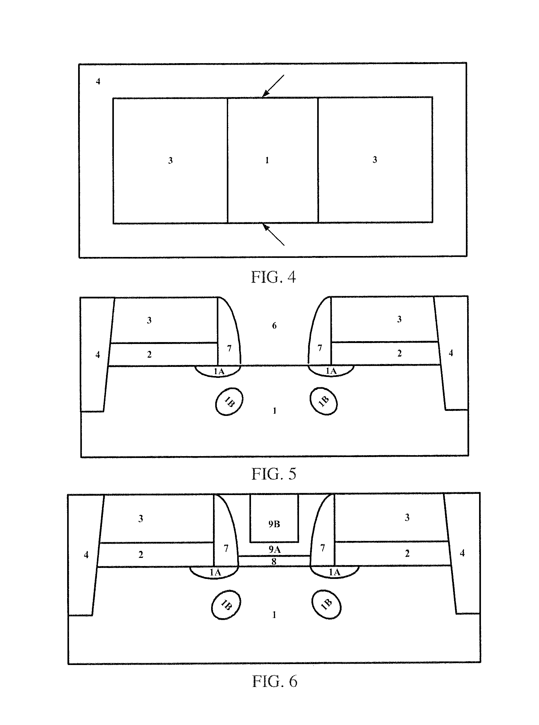
[0021]Referring to FIG. 10 and FIGS. 1 to 4, a contact sacrificial pattern is formed on the substrate, covering the source region and the drain region and exposing the gate region.
[0022]As shown in FIG. 1, a first contact sacrificial layer and a second sacrificial layer are sequentially formed on a substrate 1. The substrate 1 is provided, which may be of (bulk) Si (for example, single-crystal Si wafer), SOI, single-crys...
PUM
 Abstract
Description
Claims
Application Information