

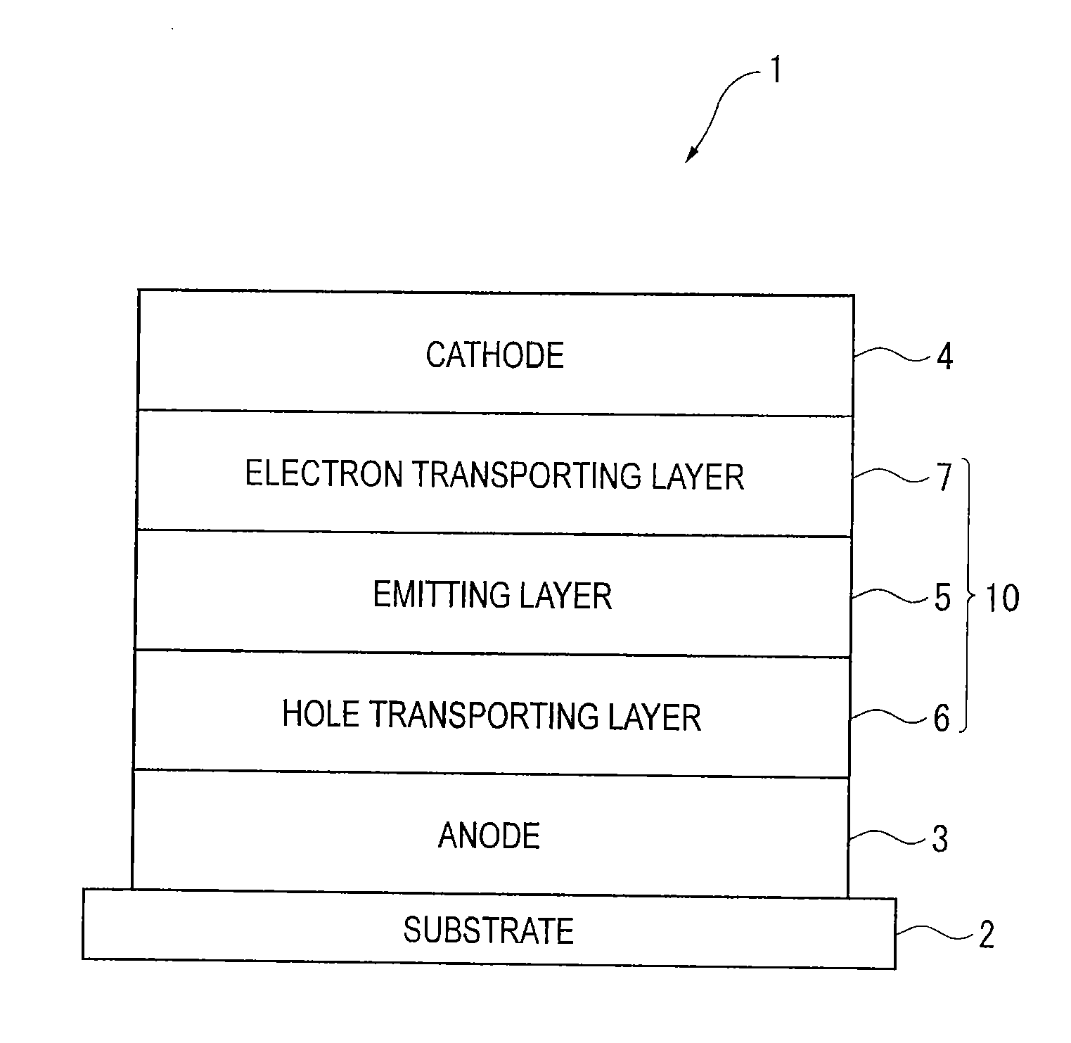
Organic electroluminescent element
a technology of electroluminescent elements and electroluminescent devices, which is applied in the direction of thermoelectric devices, triarylamine dyes, anthracene dyes, etc., can solve the problems of many practical problems in using delayed fluorescence by the tadf mechanism, and achieve the effect of reducing luminous efficiency and maximising luminous efficiency
- Summary
- Abstract
- Description
- Claims
- Application Information
AI Technical Summary
Benefits of technology
Problems solved by technology
Method used
Image

Examples
example 1
[0228]A glass substrate (size: 25 mm×75 mm×1.1 mm thick, manufactured by Geomatec Co., Ltd.) having an ITO transparent electrode (anode) was ultrasonic-cleaned in isopropyl alcohol for five minutes, and then UV / ozone-cleaned for 30 minutes. A film of ITO was 77 nm thick.
[0229]After the glass substrate having the transparent electrode line was cleaned, the glass substrate was mounted on a substrate holder of a vacuum evaporation apparatus. Initially, a compound HA-1 was deposited on a surface of the glass substrate where the transparent electrode line was provided in a manner to cover the transparent electrode, thereby forming a 5-nm thick film of the compound HA-1. The HA-1 film serves as a hole injecting layer.
[0230]After the film formation of the HA-1 film, a compound HT-1 was deposited on the HA-1 film to form a 65-nm thick HT-1 film. The HT-1 film serves as a first hole transporting layer.
[0231]A compound HT-2 was deposited on the HT-1 film to form a 10-nm thick HT-2 film. The H...
example 2
[0251]A glass substrate (size: 25 mm×75 mm×1.1 mm thick, manufactured by Geomatec Co., Ltd.) having an ITO transparent electrode (anode) was ultrasonic-cleaned in isopropyl alcohol for five minutes, and then UV / ozone-cleaned for 30 minutes. A film of ITO was 77 nm thick.
[0252]After the glass substrate having the transparent electrode line was cleaned, the glass substrate was mounted on a substrate holder of a vacuum evaporation apparatus. Initially, a compound HA-1 was deposited on a surface of the glass substrate where the transparent electrode line was provided in a manner to cover the transparent electrode, thereby forming a 5-nm thick film of the compound HA-1. The HA-1 film serves as a hole injecting layer.
[0253]After the film formation of the HA-1 film, a compound HT-1 was deposited on the HA-1 film to form a 125-nm thick HT-1 film. The HT-1 film serves as a first hole transporting layer.
[0254]A compound HT-2 was deposited on the HT-1 film to form a 25-nm thick HT-2 film. The ...
PUM
 Abstract
Description
Claims
Application Information