Glass packaging structure and glass packaging method of utilizing the same

a glass and packaging technology, applied in the field of display technology, can solve the problems of active area and transistor damage, and achieve the effects of improving the defect-free rate, poor control of the height of frit glue, and reducing the cost of operation

Active Publication Date: 2015-07-09
SHENZHEN CHINA STAR OPTOELECTRONICS TECH CO LTD
View PDF11 Cites 6 Cited by
  • Summary
  • Abstract
  • Description
  • Claims
  • Application Information

AI Technical Summary

Benefits of technology

[0008]The purpose of the present invention is to provide a glass packaging structure and a glass packaging method utilizing the same. This can be achieved by forming glass packaging lines with a specific pattern upon a packaging glass substrate by a physical or chemical etching method, making the g...

Problems solved by technology

However, the active area and transistors will be damaged by the heat generated dur...

Method used


Image

  • Glass packaging structure and glass packaging method of utilizing the same
  • Glass packaging structure and glass packaging method of utilizing the same
  • Glass packaging structure and glass packaging method of utilizing the same

Examples


first embodiment

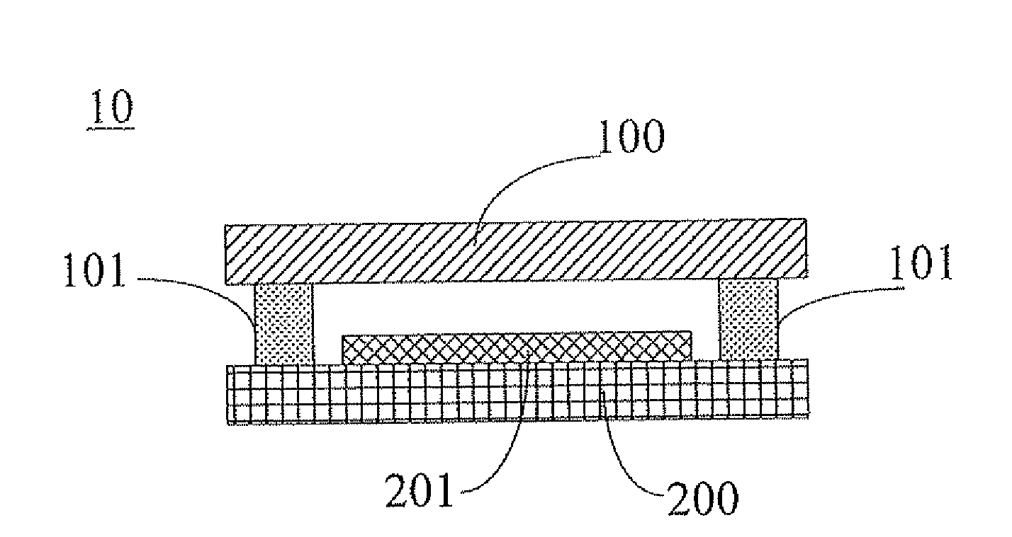
[0028]FIG. 1 is a side view drawing of a glass packaging structure of the present invention. The packaging structure comprises an active glass substrate 200 and a packaging glass substrate 100. Having an active area 201 upon the active glass substrate 200. Forming a glass packaging lines 101 with a specific pattern upon a packaging glass substrate 100. The surface of the packaging glass substrate 100 with the glass packaging lines 101 faces to the active glass substrate 200, and entirely overlapping upon the active glass substrate 200, in order to couple the packaging glass substrate 100 and the active glass substrate 200 with the packaging glass lines 101.

[0029]The glass packaging lines 101 formed upon the packaging glass substrate 100 have the same height. In particular, the glass packaging lines 101 has a height between 1-1000 μm, and glass packaging lines 101 has a width between 10-5000 μm. When disposing the packaging glass substrate 100 entirely overlapping upon the active gla...

third embodiment

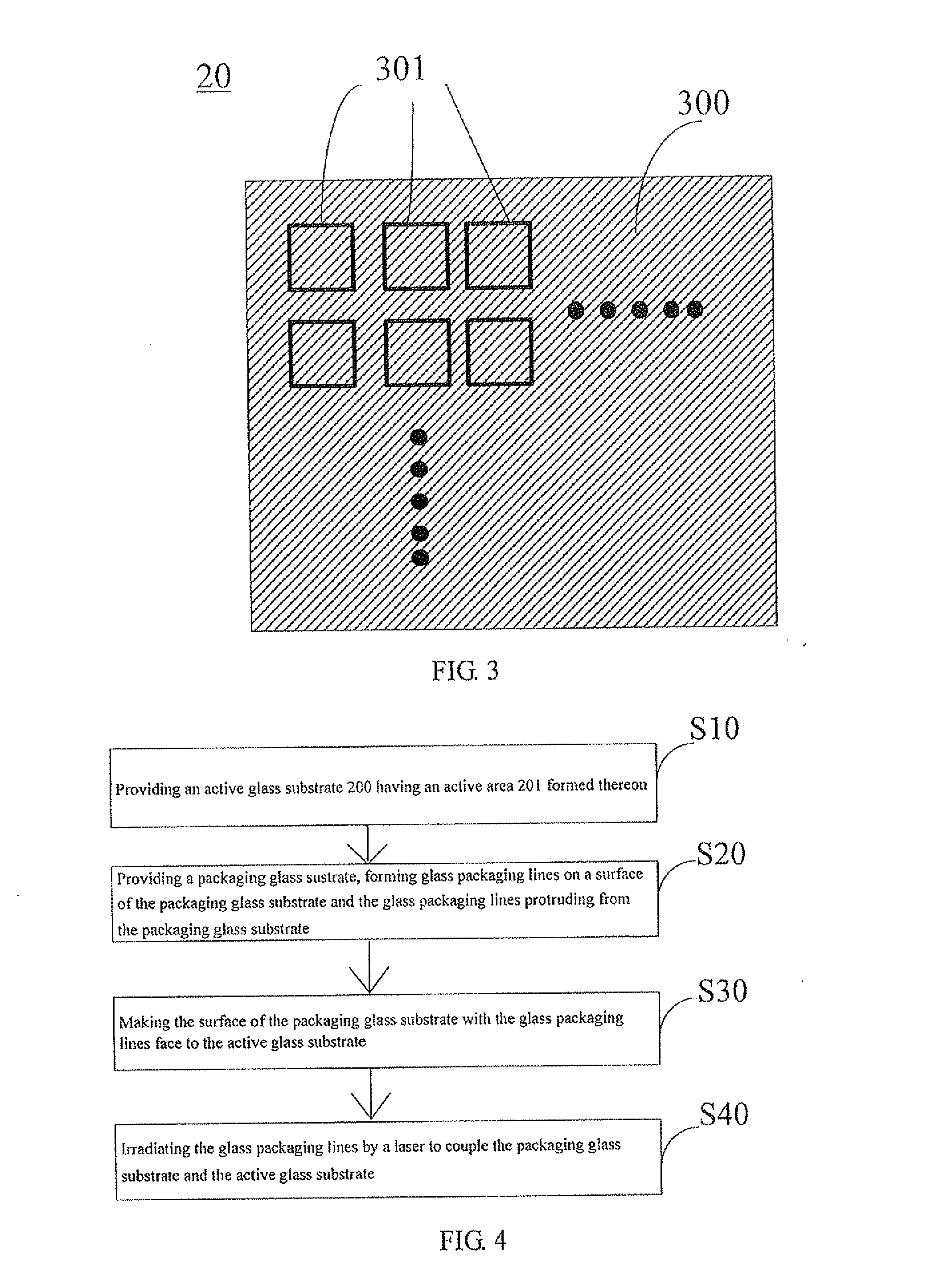
[0037]In the present invention, a circle of the UV glue 102 is coated on the glass packaging substrate 100. In particular, the position of the UV glue 102 is located outside the glass packaging lines 101. More particularly, the distance from the four sides to the UV glue 102 is between 2-10 mm.

[0038]In practice, the chamber of the combination equipment (not shown) will be filled with Nitrogen (N2), Applying a UV mask (not shown) to protect the active area 101 and TFTs (not shown), then using a UV light (not shown) to solidify the UV glue 102 having a sealing environment with N2 inside the UV glue 102, the packaging glass substrate 100 and the active glass substrate 200. Then, irradiating the glass packaging lines 101 by laser to couple the packaging glass substrate 100 and the active glass substrate 200.

[0039]FIG. 7 is a flow chart of the glass packaging method of a glass packaging structure of a third embodiment of the present invention. The combination process of the glass packagi...


PUM

PropertyMeasurementUnit
Poweraaaaaaaaaa
Distanceaaaaaaaaaa
Wavelengthaaaaaaaaaa

Abstract

The present invention provides a glass packaging structure, comprising an active glass substrate and a packaging glass substrate. An active area is formed upon the active glass substrate. Glass packaging lines are formed on a surface of the packaging glass substrate and the glass packaging lines protruding from the packaging glass substrate. The packaging glass substrate entirely overlapping upon the active glass substrate and then the glass packaging lines are irradiated by a laser to couple the packaging glass substrate and the active glass substrate.

Description

BACKGROUND OF THE INVENTION[0001]1. Field of Invention[0002]The present invention relates to a field of display technology, and more particularly, to a glass packaging structure and a glass packaging method of utilizing the same.[0003]2. Description of Prior Art[0004]In the field of display technology, liquid crystal displays / organic light emitting displays (LCD\OLED) have gradually replaced CRT displays. For the purpose of packaging the light source inside the glass substrate in an OLED, coupling two plain glass substrates is an essential technology which will direct affect the performance of the display.[0005]The earliest packaging technology applying in an LCD\OLED is ultra violet (UV) solidification packaging technology. Because an LCD is less sensitive to moisture and oxygen, the UV solidification packaging technology became the most popular packaging technology in the field of LCD packaging. The UV solidification packaging technology is coating UV glue, which will solidify aft...

Claims


Application Information

Patent Timeline
IPC IPC(8): H01L51/52C03B23/24
CPCC03B23/245H01L51/5246C03C27/10H05B33/10Y10T428/239Y02P40/57H10K50/8426
Inventor LIU, YAWEI
Owner SHENZHEN CHINA STAR OPTOELECTRONICS TECH CO LTD
Why Eureka
Try Eureka