

Display device
a display device and liquid crystal technology, applied in non-linear optics, instruments, optics, etc., can solve the problems of deterioration in image quality, difficulty in process elimination of flickering, deterioration in efficiency of liquid crystal display devices, etc., to reduce transmittance, deepen color of color filters, and expand color reproduction range
- Summary
- Abstract
- Description
- Claims
- Application Information
AI Technical Summary
Benefits of technology
Problems solved by technology
Method used
Image

Examples
first embodiment
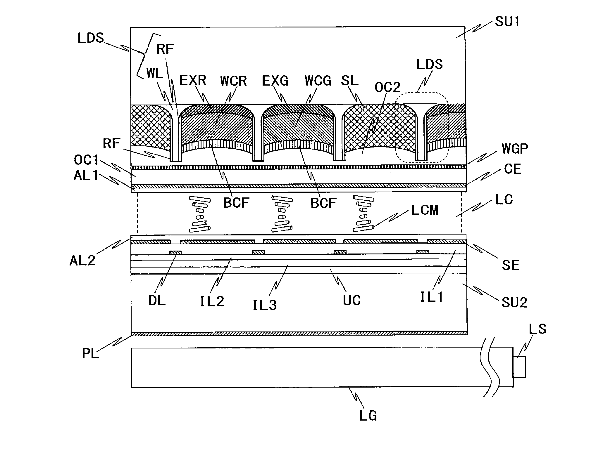
[0035]A display device (liquid crystal display device) of a first embodiment according to the present invention will be described referring to FIGS. 1 to 4, 15, 16A, 16B and 17. FIG. 1 is a sectional view of a main part of the liquid crystal display device of the embodiment, which includes three pixels of red, green and blue. The liquid crystal display device is configured to interpose a liquid crystal layer LC between a first substrate SU1 and a second substrate SU2. A first orientation film AL1, a common electrode CE, a first planarization layer OC1, a polarizing layer WGP, and a second planarization layer OC2 are sequentially laminated on the first substrate SU1 from the side adjacent to the liquid crystal layer LC. A stray light prevention layer BCF, a red wavelength conversion layer WCR, a green wavelength conversion layer WCG, a light source light scattering layer SL, a red excitation light absorbing layer EXR, and a green excitation light absorbing layer EXG are arranged into...
second embodiment
[0065]A display device of a second embodiment according to the present invention will be described referring to FIG. 5. The description which has been explained in the first embodiment may be applied to this embodiment unless otherwise special circumstances, and explanation thereof, thus will be omitted. FIG. 5 is a sectional view of a main part of the display device of the embodiment. This embodiment is different from the first embodiment in that the proximal portion (splay shape) with small inclination angle is removed from the wall-like structure WL of the light extraction structure LDS to provide only the wall surface (perpendicular shape) with the inclination angle nearly 90° as shown in FIG. 5. The cross-section of the wall-like structure WL may be obtained by selecting the highly reactive negative resist material, and adjusting the amount of exposure and development conditions for subjecting the material to the photolithography process of the material. In this embodiment, the...
third embodiment
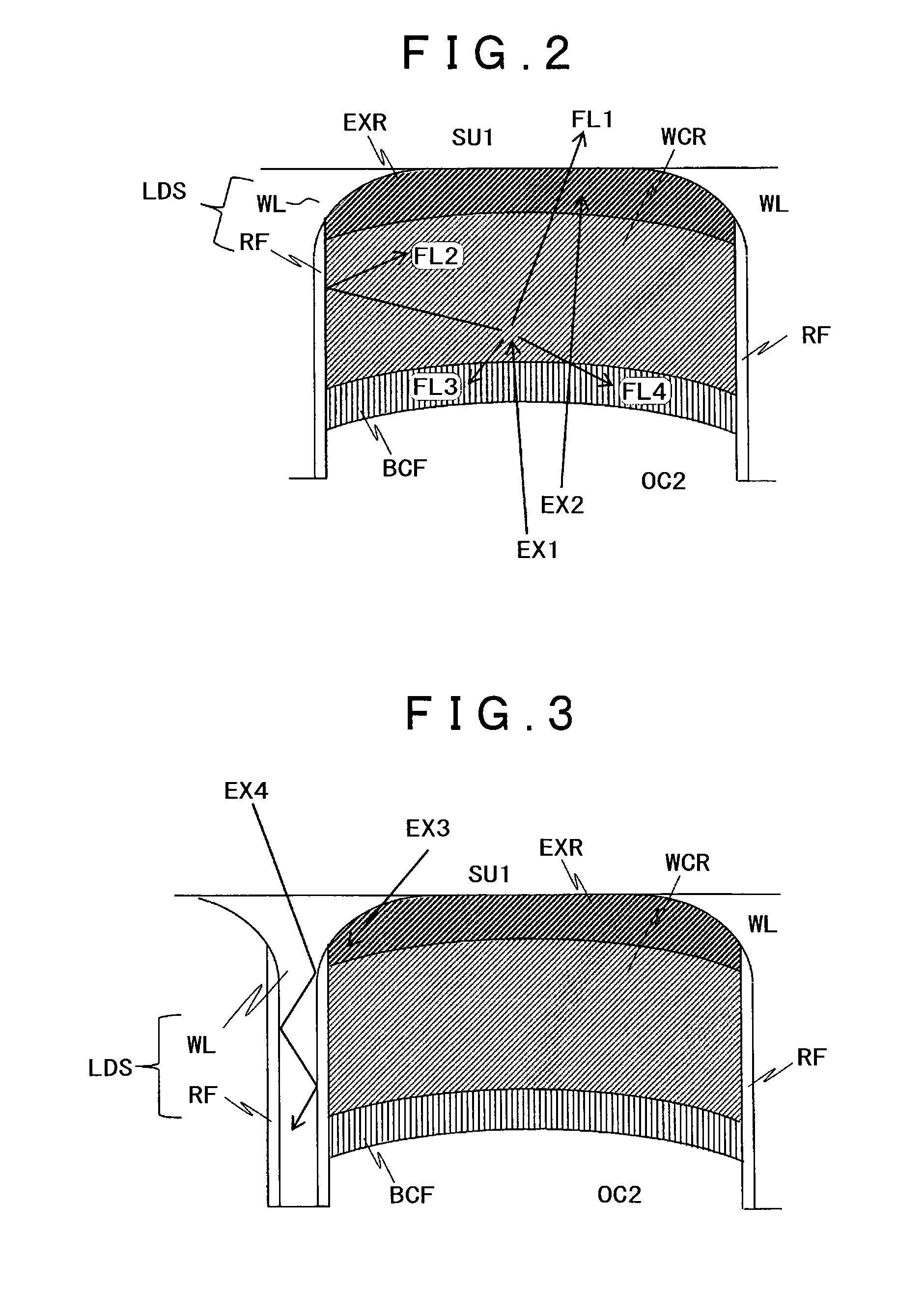
[0068]A display device of a third embodiment according to the present invention will be described referring to FIGS. 6 and 7. The description which has been explained in the first or the second embodiment may be applied to this embodiment unless otherwise special circumstances, and explanation thereof, thus will be omitted. FIG. 6 is a sectional view of a main part of the display device of the embodiment. This embodiment is different from the first embodiment in that the reflection layer RF in the light extraction structure LDS is formed only on one side of the wall-like structure WL as shown in FIG. 6. The structure may be obtained after forming the reflection layer RF in the light extraction structure LDS on both sides of the wall-like structure WL by covering only one side with the resist pattern, and removing the other side through etching.
[0069]FIG. 7 shows the typical optical path of the fluorescent light generated by the display device according to the embodiment. As the wall...
PUM
 Abstract
Description
Claims
Application Information