Device and method for bonding substrates

a technology of substrates and devices, applied in the field of devices and methods for bonding substrates, can solve the problems of complex run-out fault compensation and complex mathematical-physical description of bonding wave behavior, and achieve the effect of facilitating the deformation as claimed in the invention

Active Publication Date: 2015-07-30
EV GRP E THALLNER GMBH
View PDF2 Cites 43 Cited by
  • Summary
  • Abstract
  • Description
  • Claims
  • Application Information

AI Technical Summary

Benefits of technology

[0078]By the first substrate and/or the second substrate being fixed solely in the region of the side walls on the

Problems solved by technology

The bonding wave propagating from a non-centric contact point would reach different locations of the substrate edge at different times. The compl

Method used


Image

  • Device and method for bonding substrates
  • Device and method for bonding substrates
  • Device and method for bonding substrates

Examples


second embodiment

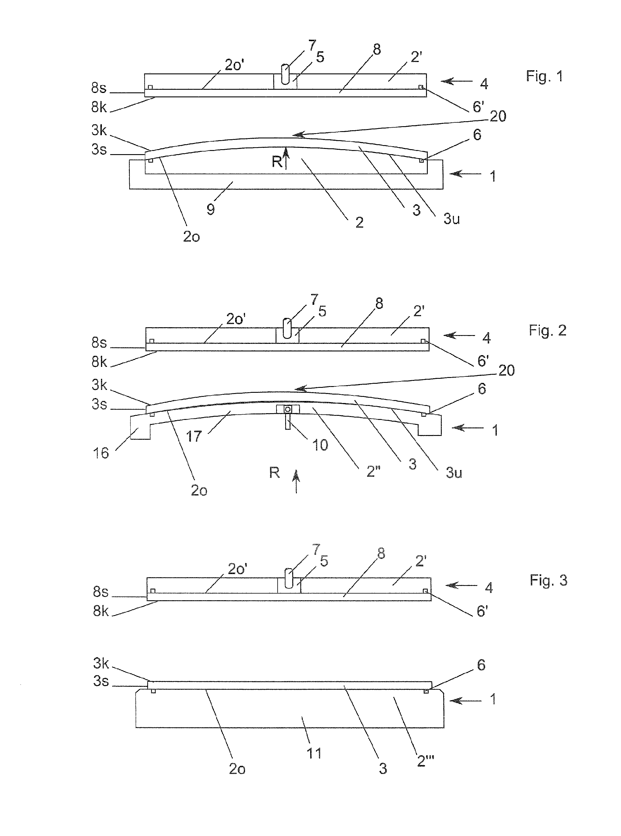
[0101]FIG. 2 shows a second embodiment with a mounting body 2″ in which the first mounting surface 2o can be deformed in a controlled manner by an actuating element 10, which in the embodiment shown is a pull rod and / or push rod. The mount 2″ has a concentrically running fixing section 16 and a deformation section 17 which encompasses the first mounting surface 2o. The deformation section 17 has at least predominantly a constant thickness and thus a predominantly constant bending stiffness. The actuating element 10 is located and fixed, on the actuating side of the deformation section 17 facing away from the mounting surface 2o. By means of the actuating element 10, the deformation section 17 can be deformed in the micrometer range and can be curved convexly and concavely. The actuating element 10 travels more than 0.01 μm, preferably more than + / −1 μm, more preferably more than + / −1 μm, still more preferably more than + / −100 μm, most preferably more than + / −1 mm, most preferably of...

third embodiment

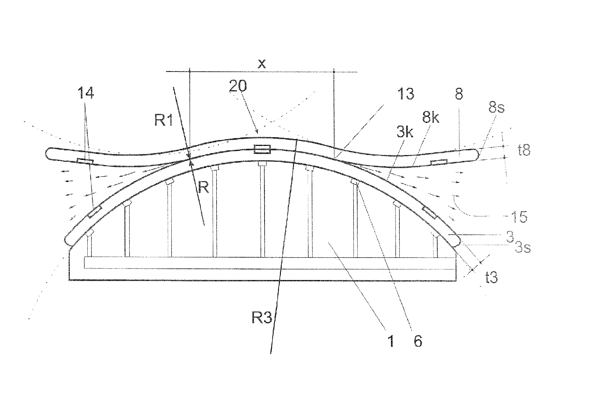
[0102]FIG. 3 shows a third embodiment with a first mounting apparatus 1 with a mounting body 2′″. The mounting body 2′″ has the first mounting surface 2o for accommodating the first substrate 3. Furthermore, the first mounting apparatus 1 in this embodiment has temperature control means 11 for temperature control (heating and / or cooling) of the mounting body 2′″ at least in the region of the first mounting surface 2o, and preferably the entire mounting body 2′″.

[0103]In the first procedure, the first substrate 3 is fixed on the heated mounting body 2′″ only after reaching its expansion which has been caused by the temperature difference. In this way, the first substrate 3 expands according to its own coefficient of thermal expansion.

[0104]In a second procedure, the first substrate 3 is fixed on the mounting body 2′″ before thermal loading by the temperature control means 11. By changing the temperature control means 11, the mounting body 2′″ and thus the first mounting surface 2o wi...

fourth embodiment

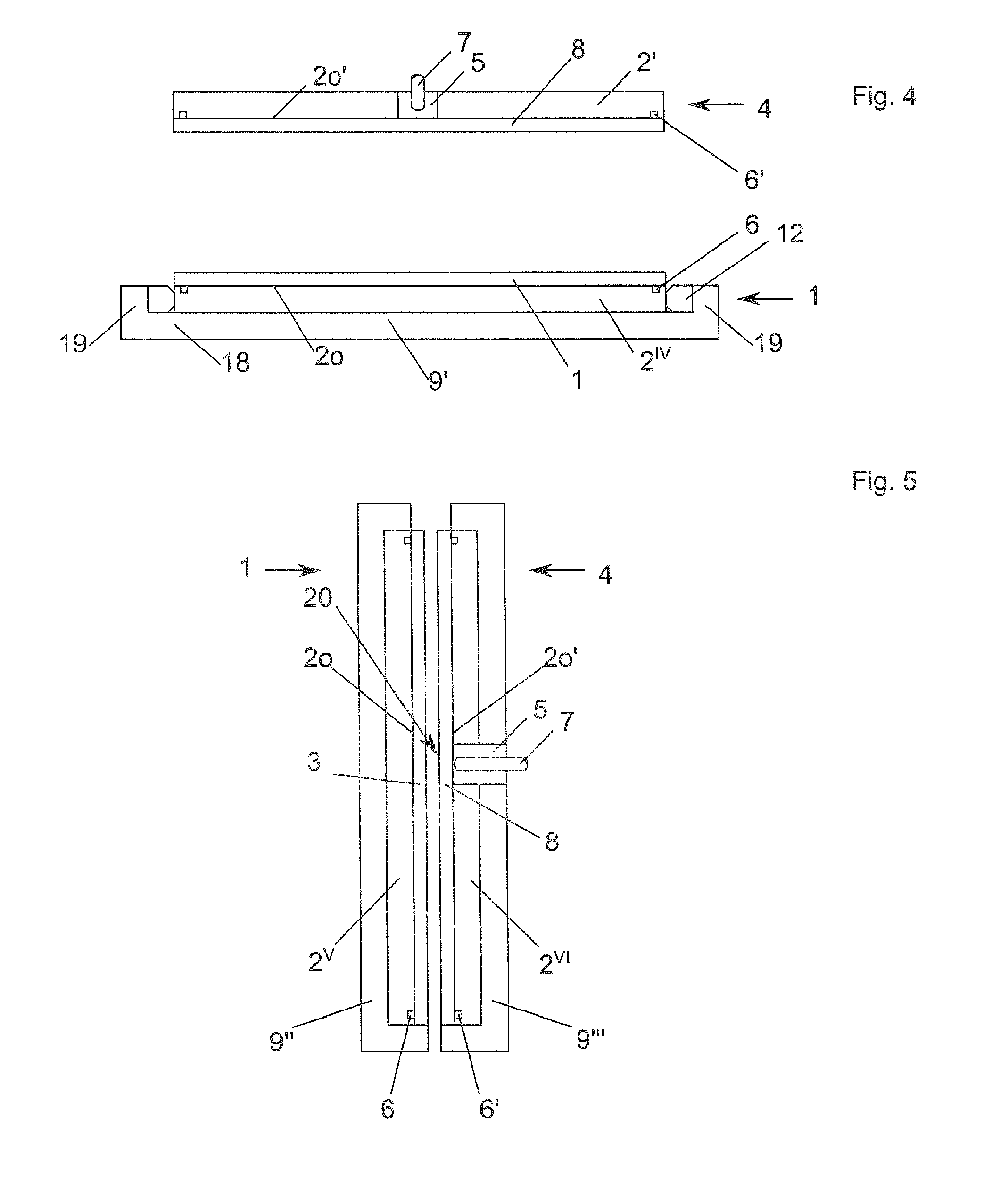
[0105]FIG. 4 shows a fourth embodiment with a base body 9′ with a mounting section 18 for accommodating a mounting body 2IV. The base body 9′ comprises a shoulder section 19 which adjoins the mounting section 18 and which is made circumferential. The shoulder section 19 is used as a stop for actuating elements 12, which are used for deformation of the mounting body 2IV in the lateral direction. The actuating elements 12 in the form of plurality of pulling and / or pushing elements 12 are arranged and distributed on the lateral periphery of the mounting body 2IV. The actuating elements 12 are used for deformation of the mounting body 2IV in the lateral direction, by mechanical expansion and / or compression, preferably in the micrometer range. The mounting body 2IV is expanded / compressed by more than 0.01 μm, preferably more than + / −1 μm, more preferably more than + / −1 μm, still more preferably more than + / −100 μm, most preferably more than + / −1 mm, most preferably of all more than + / −10...


PUM

PropertyMeasurementUnit
Diameteraaaaaaaaaa
Temperatureaaaaaaaaaa
Deformation enthalpyaaaaaaaaaa

Abstract

A method for bonding a contact surface of a first substrate to a contact surface of a second substrate comprising of the steps of: positioning the first substrate on a first receiving surface of a first receiving apparatus and positioning the second substrate on a second receiving surface of a second receiving apparatus; establishing contact of the contact surfaces at a bond initiation site; and bonding the first substrate to the second substrate along a bonding wave which is travelling from the bond initiation site to the side edges of the substrates, wherein the first substrate and/or the second substrate is/are deformed for alignment of the contact surfaces.

Description

FIELD OF THE INVENTION[0001]This invention relates to a method for bonding of a first substrate to a second substrate.BACKGROUND OF THE INVENTION[0002]Advancing miniaturization in almost all fields of microelectronics and microsystems engineering provides for a continuing development of all technologies by which the density of all type of functional units on substrates can increase. These functional units include, for example, microcontrollers, memory components, MEMS, all type of sensors or microfluid components.[0003]Techniques for increasing the lateral density of these functional units have greatly improved in recent years. In some branches of microelectronics or microsystems engineering, the improvement is to a point that a further increase of the lateral density of the functional units is no longer possible. In microchip production, the maximum possible resolution limit for structures that are produced lithographically has been achieved. In a few years, physical or technologic...

Claims


Application Information

Patent Timeline
IPC IPC(8): B32B38/18B32B37/00
CPCB32B37/0076B32B38/1833H01L21/187Y10T156/17H01L21/2007H01L24/94H01L2224/08145H01L24/80H01L2224/94H01L2224/80896H01L2224/80895H01L2224/75744H01L2224/75251H01L2224/75801H01L2224/8009H01L2224/08121H01L24/75H01L21/67092H01L21/6838H01L2224/80H01L21/68785H01L21/67098B32B2457/14B32B37/18B32B37/10B32B38/1866B29C65/7802H01L21/683B29C66/452B29C66/73141B29C65/002B32B37/003B81C1/00357B81C2201/019
Inventor WAGENLEITHNER, THOMASWIMPLINGER, MARKUSLINDNER, PAULPLACH, THOMASKURZ, FLORIAN
Owner EV GRP E THALLNER GMBH
Why Eureka
Try Eureka