Thin-film photovoltaic device with wavy monolithic interconnects

a monolithic interconnect and thin film technology, applied in the direction of computer-aided design, pv power plants, instruments, etc., can solve the problem of relatively high resistivity of the transparent front contact layer

Active Publication Date: 2015-07-30
FLISOM
View PDF4 Cites 28 Cited by
  • Summary
  • Abstract
  • Description
  • Claims
  • Application Information

AI Technical Summary

Benefits of technology

[0007]Monolithic interconnects are customarily composed in the prior art of mostly parallel scribing lines. The present invention describes a class of monolithic interconnects made of wavy scribing lines. The waviness of said monolithic interconnects in some regions of the photovoltaic module may be tuned to the zonal sheet resistivit

Problems solved by technology

A first problem in the field of thin-film photovoltaic devices is that

Method used


Image

  • Thin-film photovoltaic device with wavy monolithic interconnects
  • Thin-film photovoltaic device with wavy monolithic interconnects
  • Thin-film photovoltaic device with wavy monolithic interconnects

Examples


Embodiment Construction

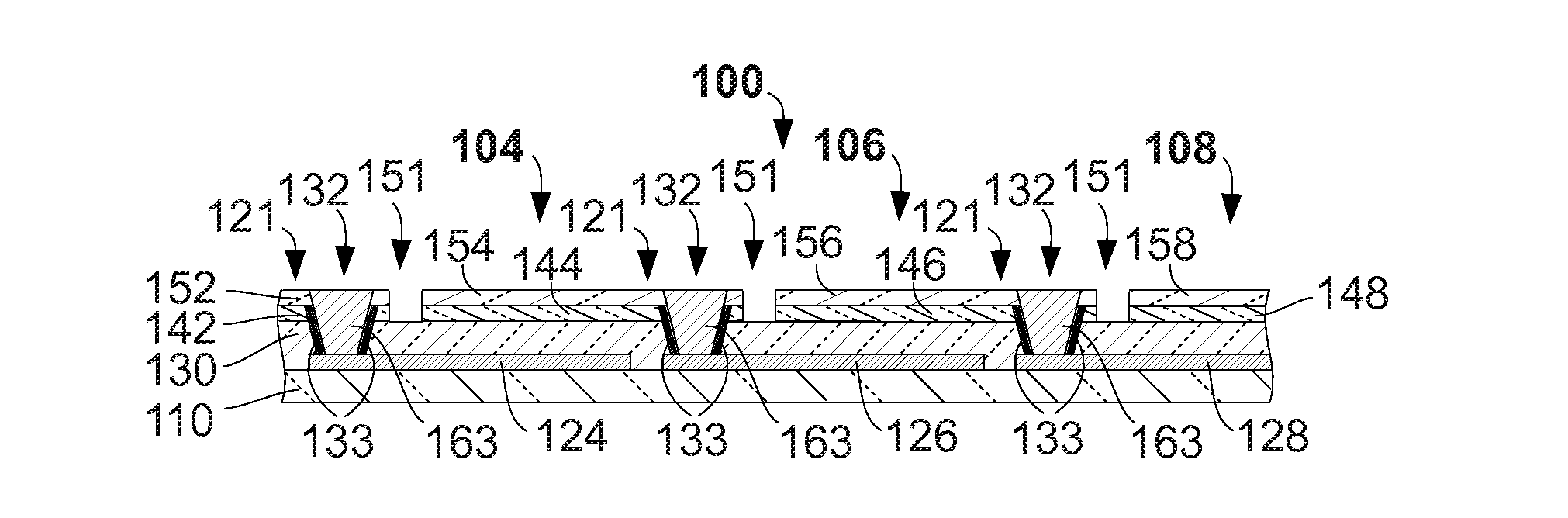
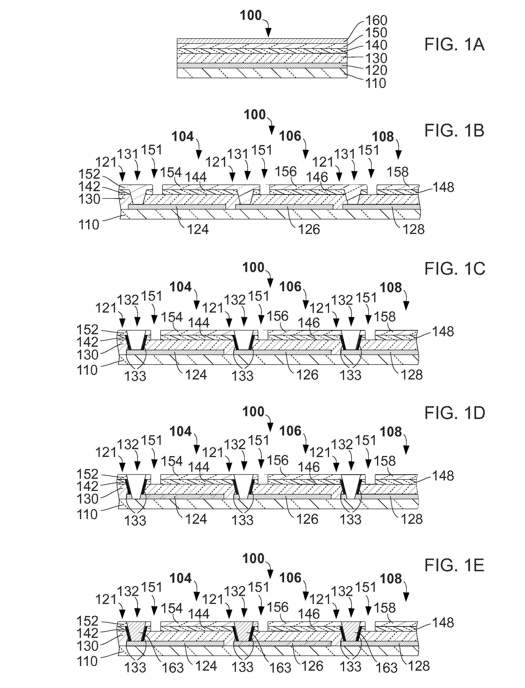
[0050]FIG. 1A shows an embodiment of a thin-film photovoltaic cell 100. FIG. 1A is represented for explanatory purposes to clarify the layer structure of a typical photovoltaic cell. A sequence of material layers is deposited on a substrate 110. Substrate 110 may be rigid or flexible and be of a variety of materials or coated materials such as glass, coated metal, plastic-coated metal, plastic, or coated plastic such as metal-coated plastic. The inventive method as described is especially advantageous for flexible materials such as plastic, metal, or flexible glass. A preferred flexible substrate material is polyimide as it is very flexible, sustains temperatures required to manufacture high efficiency optoelectronic modules, requires less processing than metal substrates, and exhibits thermal expansion coefficients that are compatible with those of material layers deposited upon it. Industrially available polyimide substrates are ordinarily available in thicknesses ranging from 7 μ...


PUM


Abstract

A thin-film optoelectronic module device (100) and design method comprising at least three monolithically-interconnected cells (104, 106, 108) where at least one monolithically-interconnecting line (250) depicts a spatial periodic or quasi-periodic wave and wherein the optoelectronic surface of said thin-film optoelectronic module device (100) presents at least one set of at least three zones (210, 220, 230) having curves of substantially parallel monolithic interconnect lines. Border zones (210, 230) have a lower front-contact sheet resistivity than th at of internal zone (220). Said curves of substantially parallel interconnecting lines may comprise peaks of triangular or rounded shape, additional spatial periods that are smaller than a baseline period, and mappings from one curve to the adjacent curve such as in the case of non-rectangular module devices (100). The device (100) and design method are advantageous to reduce costs and materials to manufacture thin-film optoelectronic module devices (100) while increasing production yield, reliability, aesthetic appearance, and range of applications.

Description

FIELD OF THE INVENTION[0001]The present invention relates to photovoltaic devices manufactured by deposition of thin-films and more particularly to the design of monolithic interconnects between cells within a photovoltaic module.BACKGROUND OF THE INVENTION[0002]Photovoltaic devices are generally understood as photovoltaic cells or photovoltaic modules. Photovoltaic modules ordinarily comprise arrays of interconnected photovoltaic cells.[0003]Thin-film photovoltaic modules, a variety of which is also known as thin-film solar modules, are generally composed of a number of electrically interconnected optoelectronic components. Such components may be optoelectronic devices such as photovoltaic cells and additional optional components such as diodes and other electronic devices.[0004]Multilayer thin-film technologies enable the monolithic integration and interconnection of several optoelectronic components and associated components on a same substrate. This integration is produced in si...

Claims


Application Information

Patent Timeline
IPC IPC(8): H01L31/05G06F17/50H01L31/02
CPCH01L31/0516G06F17/5077H01L31/0508H01L31/0201H01L31/035272Y02E10/50H01L31/0463H01L31/022433H01L31/046H01L31/0465G06F30/394
Inventor PFEIFFER, RETOZILTENER, ROGERNETTER, THOMAS
Owner FLISOM
Why Eureka
Try Eureka